Introduction
In the earlier 60’s it was discrete logic used by electronic industry. The digital system would look like noodle like maze of wiring between components. Once it is built it will be difficult to do rework on it. Sometimes the designers would forget what they have designed for! Manufacturing such systems was very difficult and redesign will be so eye-shutting just like making a PCB every time we redesign. The chip manufactures resolved this issue by placing an unconnected array of AND-OR gates in a single chip device called a programmable logic device (PLD).
The PLD contains an array of fuses that could be blown open or left closed to connect various pins to each AND gate. We can program a PLD with a set of Boolean sum-of-product equations so tat would perform the needed logic functions for our system.
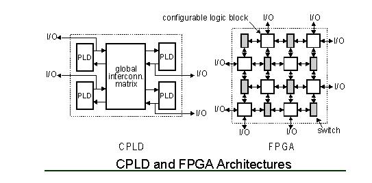
A CPLD contains a bunch of PLD blocks whose inputs and outputs are connected together by a global interconnection matrix. So a CPLD has two levels of programmability: each PLD block can be programmed, and then the interconnections between the PLDs can be programmed.
An FPGA takes a different idea. It has a clump of simple, configurable logic blocks arranged in an array with interspersed switches that can rearrange the interconnections between the logic blocks. Each logic block is individually programmed to perform a logic function (such as AND, OR, XOR, etc.) and then the switches are programmed to connect the blocks so that the complete logic functions are implemented.
Differences between FPGA and CPLD
|
FPGA |
CPLD |
| Suited for timing circuit because they have more registers. | CPLD is suited for control circuit because they have more combinational circuit. |
| Timing reports will be different if same code is synthesized many times. | Timing reports will be same result. |
| FPGA can be used to high-end product | CPLD can be used to low-end product |
| FPGA has more flexibility as well as design capacity. | CPLD has less compared to FPGA regarding design complexity |
| FPGA can operate at very high speed | CPLD has less |
| The FPGA are volatile in many cases, that’s way they need a configuration memory for working with programmed design. | CPLD devices are not volatile. They contain flash or erasable ROM memory in all of cases. |
| FPGA could not work untill the configuration is done. | The CPLD could work immediately after power up. |
| FPGA is RAM base. | CPLD is ROM base. |
| FPGAs are “fine-grain” devices. That means that they contain a lot (up to 100000) of tiny blocks of logic with flip-flops. | CPLDs are “coarse-grain” devices. They contain relatively few (a few 100’s max) large blocks of logic with flip-flops. |
| FPGAs have special routing resources to implement efficiently binary counters and arithmetic functions (adders, comparators…). CPLDs do not. | CPLDs have a faster input-to-output timings than FPGAs (because of their coarse-grain architecture, one block of logic can hold a big equation), so are better suited for microprocessor decoding logic for example than FPGAs. |
| FPGAs can contain very large digital designs | CPLDs can contain small designs only. |
Implementing a logic design with the FPGA or CPLD.
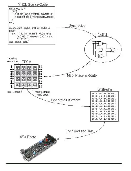
- Enter a descript_ion of the logic circuit using a hardware descript_ion language (HDL) such as VHDL or Verilog. This can also be done by drawing the design using a schematic editor.
- Use a logic synthesizer program to transform the HDL or schematic into a netlist. The netlist is a descript_ion of the various logic gates in the design and their interconnection behavior.
- Use the implementation tools to map the logic gates and interconnections into the FPGA. The configurable logic blocks in the FPGA can be further decomposed into look-up tables that perform logic operations. The CLBs and LUTs are closely linked with various routing resources. The mapping tool collects the netlist gates into groups that fit into the LUTs and then the place & route tool assigns the gate collections to specific CLBs while opening or closing the switches in the routing matrices to connect the gates together.
- Once the implementation phase is complete, a program extracts the state of the switches in the routing matrices and generates a bit stream where the ones and zeroes correspond to open or closed switches.
- The bit stream is downloaded into a physical FPGA chip (usually embedded in some larger system). The electronic switches in the FPGA open or close in response to the binary bits in the bit stream. Upon completion of the downloading, the FPGA will perform the operations specified by your HDL code or schematic. You can apply input signals to the I/O pins of the FPGA to check the operation of your design.
Credit: This article is compiled Mr.Sarath who is working as a VLSI Engineer in Nest Group of Companies.


