1. Blog>
  2. PCBWay Plug-In for KiCad

PCBWay Plug-In for KiCad

by: Apr 01,2022 60553 Views 27 Comments Posted in News

Kicad PCB design

Send your layout to PCBWay for instant production with just one click.

Have you ever thought that when you complete the design on KiCad, you can place an order on pcbway with just one click?

Now this idea is finally achieved (it's not an April Fool's joke).


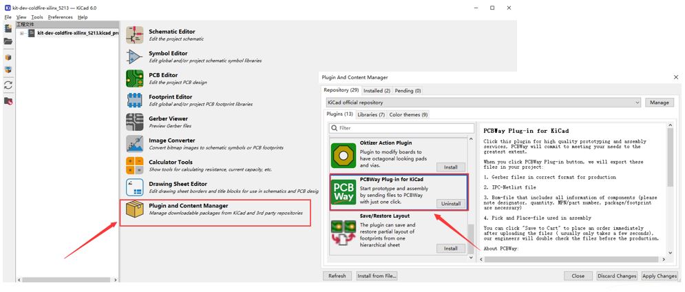
When you click PCBWay Plug-in button on Kicad, we will export these files in your project (Please make sure you have installed the latest version of the plugin released on July 11, 2024):

1.Gerber files in correct format for production

2.IPC-Netlist file

3.Bom-file that includes all information of components

4.Pick and Place-file used in assembly


You can click "Save to Cart" to place an order immediately after uploading the files( usually only takes a few seconds), our engineers will double check the files before the production.


Note:We have updated plugin for Kicad 8,you could also place assembly order directly now. But we need to get the component "Manufacture Part Number". Please confirm you run the "Update Board from Schematic" and install the latest version of the plugin.


Installation from the official KiCad repositories

Just open the "Plugin and Content Manager" from the KiCad main menu an install the "PCBWay Plug-in for KiCad" plugin from the selection list.

Manual installation

You can also download the latest ZIP file from https://github.com/pcbway/PCBWay-Plug-in-for-Kicad, then open the "Plugin and Content Manager" from the main window of KiCad and install the ZIP file via "Install from File".


About Bom

We can get all information of components used in your design (please make sure you have installed the latest version of the plugin). In order to speed up the quotation of components, we need this information:

1. Designator (necessary)

2. Quantity (necessary)

3. MPN/Part Number (necessary)

4. Package/Footprint (necessary)

5. Manufacturer (optional)

6. Description/value (optional)


You just need to add the properties in your schematic like the picture shows:


As a sponsor of KiCad, we will always support its development.


Note:Thanks to the open source community. Since we are not skilled enough to edit on github at the moment, any feedback or questions please contact with anson@pcbway.com

Join us
Wanna be a dedicated PCBWay writer? We definately look forward to having you with us.
  • Comments(27)
Upload photo
You can only upload 5 files in total. Each file cannot exceed 2MB. Supports JPG, JPEG, GIF, PNG, BMP
0 / 10000
  • Having a direct PCBWay plug-in will definitely streamline the ordering process and improve efficiency.
    <a href="https://google.com/">google</a>

    Reply
  • What are the differences between this plug-in and the "PCBWay Fabrication Toolkit" plug-in?

    PCBWay Team 2024-09-26 09:59:22Reply

    The PCBWay Plug-in for KiCad directly redirects you to our pricing page to upload production files, while the PCBWay Fabrication Toolkit generates production files locally. You can install both and check their corresponding features.

    Reply
  • Dear PCBWay Team, are there any news on this topic? This "bug" gives us some headaches when ordering new PCBs

    PCBWay Team 2024-06-04 09:59:32Reply

    Hello, thanks for your feedback. Our colleagues will contact you.

    Reply
  • This is the updated script_ that does not saves in the BOM parts with "Exclude from bill of materials" Also it checks for Package or Pack field and saves that information in BOM, only if it cannot find this field it saves the Footprint as a package #https://opensource.org/licenses/MIT import os import json import csv import re from .config import * class PCBWayProcess: def __init__(self): self.board = pcbnew.GetBoard() self.pctl = pcbnew.PLOT_CONTROLLER(self.board) self.bom = [] self.components = [] def get_gerber_file(self, temp_dir): settings = self.board.GetDesignSettings() settings.m_SolderMaskMargin = 0 settings.m_SolderMaskMinWidth = 0 #pctl = pcbnew.PLOT_CONTROLLER(self.board) popt = self.pctl.GetPlotOptions() popt.SetOutputDirectory(temp_dir) popt.SetPlotFrameRef(False) popt.SetSketchPadLineWidth(pcbnew.FromMM(0.1)) popt.SetAutoScale(False) popt.SetScale(1) popt.SetMirror(False) popt.SetUseGerberAttributes(True) if hasattr(popt, "SetExcludeEdgeLayer"): popt.SetExcludeEdgeLayer(True) popt.SetUseGerberProtelExtensions(False) popt.SetUseAuxOrigin(True) popt.SetSubtractMaskFromSilk(True) popt.SetDrillMarksType(0) # NO_DRILL_SHAPE for layer_info in plotPlan: if self.board.IsLayerEnabled(layer_info[1]): self.pctl.SetLayer(layer_info[1]) self.pctl.OpenPlotfile( layer_info[0], pcbnew.PLOT_FORMAT_GERBER, layer_info[2]) self.pctl.PlotLayer() self.pctl.ClosePlot() def get_netlist_file(self, temp_dir): drlwriter = pcbnew.EXCELLON_WRITER(self.board) drlwriter.SetOptions( False, True, self.board.GetDesignSettings().GetAuxOrigin(), False) drlwriter.SetFormat(False) drlwriter.CreateDrillandMapFilesSet(self.pctl.GetPlotDirName(), True, False) netlist_writer = pcbnew.IPC356D_WRITER(self.board) netlist_writer.Write(os.path.join(temp_dir, netlistFilename)) def get_components_file(self, temp_dir): if hasattr(self.board, 'GetModules'): footprints = list(self.board.GetModules()) else: footprints = list(self.board.GetFootprints()) footprints.sort(key=lambda x: x.GetReference()) for i, f in enumerate(footprints): try: footprint_name = str(f.GetFPID().GetFootprintName()) except AttributeError: footprint_name = str(f.GetFPID().GetLibItemName()) layer = { pcbnew.F_Cu: 'top', pcbnew.B_Cu: 'bottom', }.get(f.GetLayer()) f_attrs = f.GetAttributes() parsed_attrs = self.parse_attrs(f_attrs) mount_type = 'smt' if parsed_attrs['smd'] else 'tht' placed = not parsed_attrs['not_in_bom'] rotation = f.GetOrientation().AsDegrees() if hasattr(f.GetOrientation(), 'AsDegrees') else f.GetOrientation() / 10.0 designator = f.GetReference() pos_x = (f.GetPosition()[0] - self.board.GetDesignSettings().GetAuxOrigin()[0]) / 1000000.0 pos_y = (f.GetPosition()[1] - self.board.GetDesignSettings().GetAuxOrigin()[1]) * -1.0 / 1000000.0 mpn = self.get_mpn_from_footprint(f) pack = self.get_pack_from_footprint(f) if pack: footprint_name = pack value = f.GetValue() self.components.append({ 'pos_x': pos_x, 'pos_y': pos_y, 'rotation': rotation, 'side': layer, 'designator': designator, 'mpn': mpn, 'pack': footprint_name, 'value': value, 'mount_type': mount_type, 'place': placed }) is_exist_bom = False for exist_bom in self.bom: if exist_bom['mpn'] == mpn and exist_bom['pack'] == footprint_name and exist_bom['value'] == value: exist_bom['designator'] += ', ' + designator exist_bom['quantity'] += 1 is_exist_bom = True if is_exist_bom == False and placed == True: self.bom.append({ 'designator': designator, 'quantity': 1, 'value': value, 'pack': footprint_name, 'mpn': mpn, 'mount_type': mount_type }) if len(self.components) > 0: with open((os.path.join(temp_dir, positionsFilename)), 'w', newline='', encoding='utf-8-sig') as outfile: csvobj = csv.writer(outfile) csvobj.writerow(self.components[0].keys()) for component in self.components: if ('**' not in component['designator']): csvobj.writerow(component.values()) if len(self.bom) > 0: with open((os.path.join(temp_dir, bomFilename)), 'w', newline='', encoding='utf-8-sig') as outfile: csvobj = csv.writer(outfile) csvobj.writerow(self.bom[0].keys()) for component in self.bom: if ('**' not in component['designator']): csvobj.writerow(component.values()) def get_gerber_parameter(self): boardWidth = pcbnew.ToMM(self.board.GetBoardEdgesBoundingBox().GetWidth()) boardHeight = pcbnew.ToMM(self.board.GetBoardEdgesBoundingBox().GetHeight()) if hasattr(self.board, 'GetCopperLayerCount'): boardLayer = self.board.GetCopperLayerCount() gerberData = {'boardWidth':boardWidth,'boardHeight':boardHeight,'boardLayer':boardLayer} return gerberData def get_name(self): p_name = self.board.GetFileName() return p_name def parse_attrs(self, attrs): return {} if not isinstance(attrs, int) else { 'tht': self.parse_attr_flag(attrs, pcbnew.FP_THROUGH_HOLE), 'smd': self.parse_attr_flag(attrs, pcbnew.FP_SMD), 'not_in_pos': self.parse_attr_flag(attrs, pcbnew.FP_EXCLUDE_FROM_POS_FILES), 'not_in_bom': self.parse_attr_flag(attrs, pcbnew.FP_EXCLUDE_FROM_BOM), 'not_in_plan': self.parse_attr_flag(attrs, pcbnew.FP_BOARD_ONLY) } def get_mpn_from_footprint(self, f): keys = ['mpn', 'MPN', 'Mpn', 'PCBWay_MPN' ,'part number', 'Part Number', 'Part No.', 'Mfr. Part No.', 'Mfg Part'] for key in keys: try: if f.HasField(key): return f.GetFieldByName(key).GetText() except Exception as e: if f.HasProperty(key): return f.GetProperty(key) def get_pack_from_footprint(self, f): keys = ['pack', 'PACK', 'Pack', 'package' ,'PACKAGE', 'Package', 'case', 'CASE', 'Case'] for key in keys: try: if f.HasField(key): return f.GetFieldByName(key).GetText() except Exception as e: if f.HasProperty(key): return f.GetProperty(key) def parse_attr_flag(self, attr, mask): return mask == (attr & mask)

    PCBWay Team 2024-03-19 11:52:20Reply

    Thanks for your feedback,our engineer team is checking it and will back to you soon

    Reply
  • The plugin ignores the component attributes "Do not populate" and "Exclude from Bill of Materials". Even if both are set, the component is in the generated BOM and mounted by your assembly service.

    PCBWay Team 2024-03-14 13:45:16Reply

    Our colleague will contact with you about the details

    Reply
  • I am getting an error with your plugin in KiCad 8. Errno 13 - pemission denied on the gerber.zip. Please help

    PCBWay Team 2024-03-11 10:33:42Reply

    I tried Kicad 8.0 plugin and goes well in our side,could you send your file to anson@pcbway.com. He will help check it

    Reply
  • Please add and option to select flex print or other types, the plugin is useless if you want to make anything but standard pcb.

    PCBWay Team 2024-02-02 09:15:00Reply

    Thanks for your feedback. Currently, for Flex/Rigid-Flex board design, after you click the kicad plug-in icon, you can select FPC/Rigid-Flex on the pricing page, fill in the relevant parameters, and then place an order.

    Reply
  • I have a completed circuit board design that I need to have etched. It's a small, single layer board 49mm x 15mm. How would I go about having you make that for me? ( Here's what it looks like. I need to add the holes from another layer which I have in photoshop)

    PCBWay Team 2023-10-13 09:37:25Reply

    Hello,you need to export the Gerber file from your design, then you can use this link to upload your Gerber file and place your order. https://www.pcbway.com/QuickOrderOnline.aspx. If you have any other questions, you can contact the sales representative in the upper right corner of your backend homepage.

    Reply
  • Seems like the placed filend in PCBWay_components.json is not correct. Seems to ignore the Do not populate attribute in the schematics.

    PCBWay Team 2023-08-14 15:28:25Reply

    Thanks for your feedback, our IT engineer will check it.

    Reply
  • I installed the plugin in Kicad nightly builds, and it does not seem to run. This is on Linux Mint 21.1 Regards, rob Oudendijk

    PCBWay Team 2023-08-09 09:07:55Reply

    Hello, thanks for your feedback, our IT engineer will check it.

    robouden 2023-08-14 00:14:08Reply

    Thanks

    Reply
  • This sounded sooo cool. So, I installed it and I verified that the plugin is indeed installed. Problem is, also after restarting Kicad, I can't seem to find the button anywhere. You mention the button, but you have no screenshot of where to locate it. Hope you can help :-)

    Jarl Gjessing 2023-02-07 14:17:56Reply

    Sorry, part of the video, just went on too fast. But the button is not there :-(

    PCBWay Team 2023-07-20 14:52:28Reply

    Now do you find it? We just update plugin for Kicad 7.0

    Reply
  • Hi, I'm having trouble with the plugin, can you help? I'm on KiCad 6.0.7, and when I run the plugin, the zip file is created, PCBWAY_components.json. However, the MPN data is not being included in the json file, everything is marked as null. I had this work once before but now seemingly not working anymore. Please help if you can. Thanks.

    PCBWay Team 2022-08-04 15:50:17Reply

    We will check it and back to you soon.

    Reply
  • Sounds great!

    Reply
  • I saw it by chance, it's a very good and facilitating plug-in. Thank you... 🙏

    Reply
Back to top