When it comes to surface-mounted components for highly sensitive computer parts, connecting integrated circuits via wires can be complex and challenging. In such cases, the ball grid array (BGA) is the best solution. In order to give more people a preliminary understanding of BGA, this article will provide a detailed introduction to the basic information related to BGA.
What is Ball Grid Array?
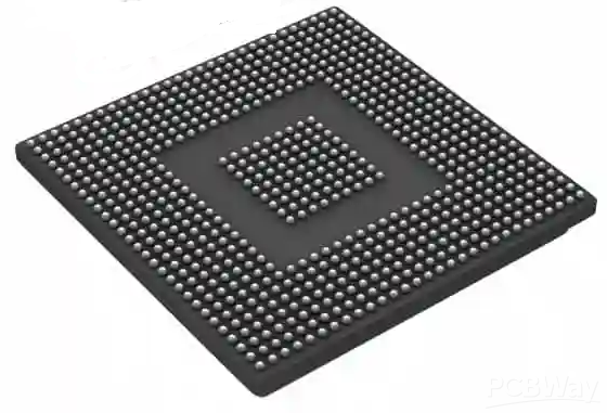
BGA is the abbreviation for Ball Grid Array. Generally speaking, it is a collection of small, tiny metal conductor balls that are regularly arranged on the circuit board during the manufacturing process of a printed circuit board (PCB).
The Ball Grid Array (BGA) employs a different connection strategy compared to ordinary surface mount connectors. Common packages, such as Quad Flat Package (QFP), place the connectors on the sides of the package. This results in limited space for the pins and the pins must be closely spaced to provide the necessary communication. However, BGA uses the bottom of the package, which ensures sufficient space for connections.
Reason for the Use of BGA
- Ball grid arrays are highly utilized in SMD ICs that require dense connections. Using the bottom surface of the IC package instead of connecting devices around the edges can reduce connection density, making PCB layout more convenient.
- Originally, using the bottom of the chip for soldering would make the entire soldering process very challenging. However, with the help of mainline PCB production equipment, these challenges can be easily overcome, ensuring the overall reliability and performance of BGA.
- Heat is the first factor to consider. BGA's superior heat dissipation performance keeps the chip at a lower temperature during operation, thereby extending the product's lifespan.
- The second factor to consider is electrical characteristics. BGA can achieve the smallest feasible resistance path. This shortest-distance connection increases the value and importance of BGA.
- The third most important factor is compatibility. Handling a large number of balls while utilizing the shortest space allows designers to have many feasible choices, thereby increasing the product's value.
Advantages of BGA
- BGA allows connections to be made underneath the SMD package rather than just around its perimeter, maximizing the utilization of PCB space.
- Enhanced thermal and electrical performance. BGA packages can provide low-inductance power and ground planes, controlled impedance routing for signal traces, and the ability to dissipate heat through the pads.
- Improved soldering increases yield; BGA allows for wider connection spacing and greater solderability.
- Reduced package thickness, which is advantageous when some devices, such as mobile phones, need to be relatively thin.
- Larger pad sizes improve reworkability.


