In modern electronic devices, high-power power supplies provide stable and reliable power for servers, electric vehicle chargers, and various industrial equipment, ensuring that the devices operate properly. The PCB plays a crucial role in the signal and power transmission between electronic components, and its design and functionality directly affect the power supply’s performance and reliability. This article will introduce key considerations in designing high-power power supply PCBs, which can effectively help create stable and efficient power circuits.
Thermal Management
- Increase Copper Layer Thickness: Using thicker copper layers can reduce conductor resistance and decrease heat generation.
- Design Heat Dissipation Holes and Thermal Channels: Properly layout heat dissipation holes and thermal channels to improve heat dissipation efficiency, allowing heat to dissipate quickly.
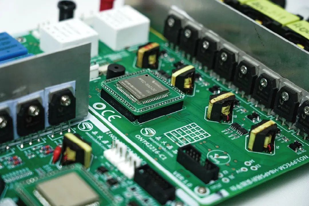
- Use Heat Sinks and Cooling Fins: Attach heat sinks directly to heat-generating components, such as power devices, to conduct heat to the cooler via welding or thermal adhesive. For particularly high-power components, add external cooling fins to enhance heat dissipation.
- Properly Layout Heat-Generating Components: When placing heat-generating and high-power components on the PCB, ensure they are positioned away from heat-sensitive components and evenly distributed across the board to prevent excessive heat concentration.
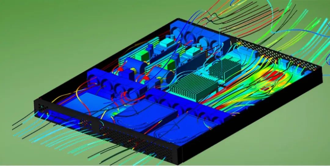
- Conduct Thermal Simulation: Use thermal simulation tools, such as ANSYS or Flotherm, to predict and analyze heat dissipation during the design phase, optimizing layout and cooling.
Power and Ground Plane Design
- Use Large Power Planes: Reduce power noise and voltage drop, improving the stability of the power supply.
- Adopt Continuous Ground Planes: Lower ground loop impedance and reduce electromagnetic interference to ensure the stability of the circuit.
Routing Design
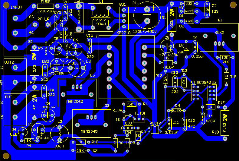
- Increase Trace Width: Design wider traces for high-current paths to reduce resistance and heat generation. The trace width can generally be calculated based on the current size to ensure it can handle the corresponding current load.
- Shorten Trace Length: Traces should be as short and direct as possible to reduce resistance and inductance, improve efficiency, and reduce power loss, especially for high-current and high-frequency signal traces.
- Avoid Parallel Routing: When routing on two-layer boards, the traces should be perpendicular, diagonal, or curved to each other, avoiding parasitic coupling caused by parallel routing.
- Proper Via Placement: Determine the size and number of vias based on current requirements and manufacturing process specifications, avoiding vias that are too small or too large. The same number of vias should be placed in the input and output circuits, and vias should be positioned appropriately. For example, vias for the input side should be placed before the capacitors, while vias for the output side should be placed after the capacitors.
Component Layout
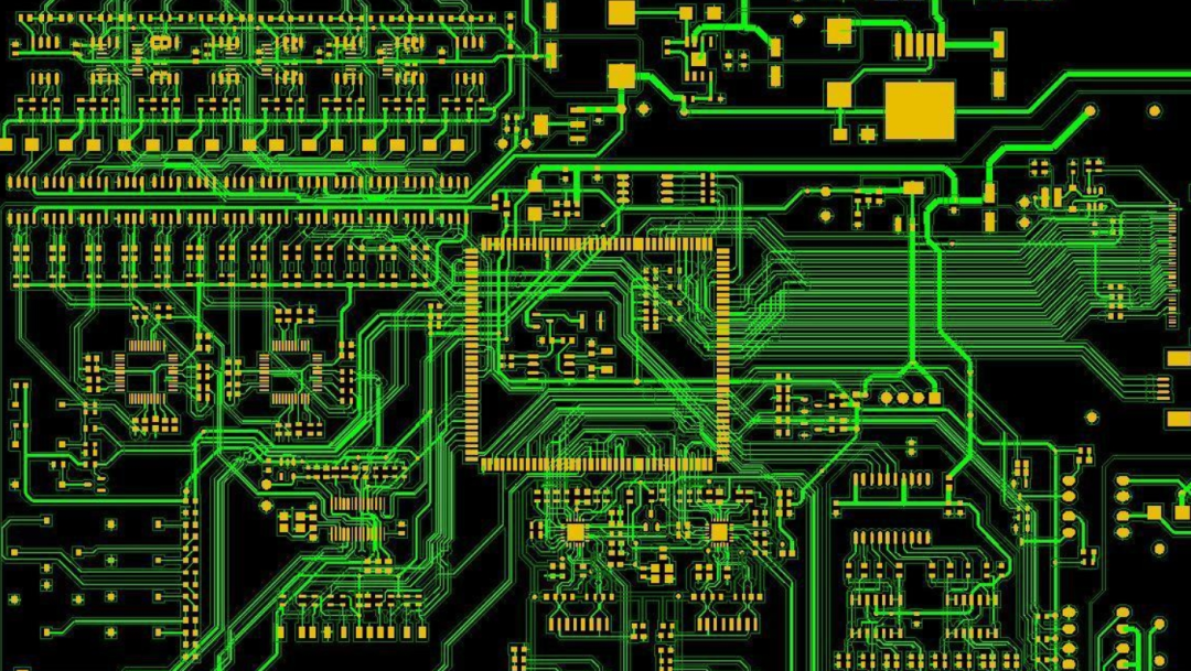
- Layout by Function Module: Group related circuits with similar functions into a single functional module. Components should be as concentrated as possible to facilitate routing and debugging. Digital circuits should be separated from analog circuits to reduce mutual interference.
- Keep Away from Sensitive Components: High-power components should be placed away from components sensitive to electromagnetic interference, such as clock chips and small-signal amplifiers, to prevent high-power signals from interfering with them.
- Consider Air Convection: On boards with thermal convection, pay attention to the layout of large passive components to avoid obstructing air convection around chips and MOSFETs.
Insulation and Safety Design
- Enhance Electrical Insulation: Use high-insulation materials and appropriate layouts to prevent interference between high-power signals and other sensitive signals. For high-voltage areas, ensure adequate insulation spacing to avoid safety hazards such as breakdown and leakage.
- Design Protection Circuits: Design overcurrent, overvoltage, and short-circuit protection circuits to prevent equipment overload or damage, ensuring the safety of both users and equipment. Install fuses on all outputs leaving the PCB, as well as an input fuse. The fuse's rated current should be lower than the current the wiring and PCB traces can handle.
- Avoid Signal Crossing: The routing design under the transformer should consider avoiding the crossing of high-voltage and low-voltage signals to reduce risks.
Electromagnetic Compatibility Design
- Reasonable Grounding Design: The ground wire should be as wide as possible to reduce current density, decrease resistance, and improve conductivity. At the same time, care should be taken to avoid ground loops to prevent the formation of magnetic fields that could affect electromagnetic compatibility.
- Electromagnetic Shielding: Install shielding covers on components prone to electromagnetic radiation, such as power coils and filters, to minimize electromagnetic radiation. For some sensitive signal lines, shielded cables can also be used for transmission to enhance anti-interference capability.
- Filtering: Add appropriate filters, such as LC filters and RC filters, to filter high-frequency noise in the power supply and reduce electromagnetic interference.
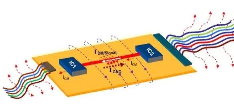
Image sourced from the internet.
If you need PCB Design/Layout,please submit youre request here:
https://www.pcbway.com/order/QuoteLayout?designType=2


