Silkscreen standards in PCB technology are a critical aspect of ensuring the quality of circuit boards and assembly efficiency. Silkscreen, which refers to the printed text and graphics on a PCB, is primarily used to identify component positions, polarity, orientation, and provide necessary manufacturing information. Below is a detailed explanation of PCB silkscreen standards and requirements:
- Silkscreen for components, mounting holes, and positioning holes: To facilitate installation and identification, all components, mounting holes, and positioning holes should have corresponding silkscreen. For example, mounting holes are typically numbered as H1, H2, etc., so that workers can follow the sequence during operation.
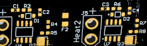
- Silkscreen character orientation: Silkscreen characters should follow the basic principles of left-to-right and bottom-to-top to maintain visual consistency. Additionally, for polarized components such as electrolytic capacitors and diodes, the direction should be consistent within the same functional unit to reduce assembly errors.
- Silkscreen treatment for pads and solder traces: There should be no silkscreen on component pads and solder traces that require soldering, to ensure the reliability of the soldering process and the continuity of the solder trace. Additionally, designators should not be covered by installed components to facilitate future installation and maintenance.
- Silkscreen for polarized components: For polarized components such as capacitors and diodes, their polarity should be clearly marked on the silkscreen to ensure easy identification and prevent reverse installation.
- Directional connectors: The silkscreen for connectors should indicate the correct insertion direction to prevent installation errors.
- Board name, date, version number, and other information: The silkscreen for this information should be clear and prominent to assist in recording and identifying different versions of the PCB.
- Manufacturer information and ESD markings: The PCB should include the manufacturer’s complete information and ESD (Electrostatic Discharge) markings when necessary to ensure safety and compliance.
- Completeness of Gerber files: Gerber files should include all necessary layers, such as the routing layer, silkscreen layer, solder mask layer, etc., to ensure manufacturing accuracy.
- Consistency of designators: The designators on the PCB must match them in the Bill of Materials (BOM) to ensure consistency between the design and the BOM.
The importance of silkscreen design standards lies in ensuring clear identification and proper installation of components, which enhances assembly efficiency and reduces errors. Well-designed silkscreen markings, such as designators, polarity indicators, and connector orientations, are essential for accurate assembly and maintenance. Additionally, proper silkscreen placement avoids interference with soldering processes and helps in the identification of PCB versions and manufacturers. Adhering to these standards improves the overall reliability and quality of the PCB, ensuring smooth production and maintenance workflows.


For connectors with polarity, the silk screen should clearly indicate the positive and negative poles to avoid wrong connection.