Danko Bertović
CROATIA • + Follow
Edit Project
Description
Universal PCB
This is PCB board that can be used for many electronic projects. With this board you can make cool project very fast. And project looks much better than perfboard projects. It is also great for SMD components because the lines are not isolated so you can solder directly to them. For 16 US dollars you will get 5 PCB boards.
?
May 15,2020
3,719 views
end-flag
Universal PCB
2 Layers PCB 80 x 60 mm FR-4, 1.6 mm, 1, HASL with lead, Black Solder Mask, White silkscreen
This is PCB board that can be used for many electronic projects. With this board you can make cool project very fast.
3719
7
1
8.75 (1)
Published: May 15,2020
Purchase
Donation Received ($)
PCBWay Donate 10% cost To Author
*PCBWay community is a sharing platform. We are not responsible for any design issues and parameter issues (board thickness, surface finish, etc.) you choose.
Copy this HTML into your page to embed a link to order this shared project
Copy
Under the
Attribution-ShareAlike (CC BY-SA)
License.

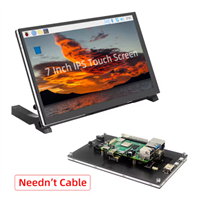
Raspberry Pi 5 7 Inch Touch Screen IPS 1024x600 HD LCD HDMI-compatible Display for RPI 4B 3B+ OPI 5 AIDA64 PC Secondary Screen(Without Speaker)
BUY NOW
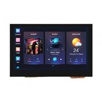
ESP32-S3 4.3inch Capacitive Touch Display Development Board, 800×480, 5-point Touch, 32-bit LX7 Dual-core Processor
BUY NOW
Raspberry Pi 5 7 Inch Touch Screen IPS 1024x600 HD LCD HDMI-compatible Display for RPI 4B 3B+ OPI 5 AIDA64 PC Secondary Screen(Without Speaker)
BUY NOW- Comments(1)
- Likes(7)
 Log in to post comments.
Upload photo
0 / 10000
It looks like you have not written anything. Please add a comment and try again.
You can upload up to 5 images!
Image size should not exceed 2MB!
File format not supported!
 Silvano Rossi
 May 31,20200 CommentsReply
-
 Engineer
Sep 15,2024
-
 Engineer
May 04,2024
-
 Felix
May 16,2023
-
 Arad Eizen
Jun 07,2020
-
 Silvano Rossi
May 31,2020
-
 AIVAS
May 24,2020
-
 Mark Wu
May 23,2020
View More
VOTING
1 votes
- 1 USER VOTES
8.75
- YOUR VOTE 0.00 0.00
- 1
- 2
- 3
- 4
- 5
- 6
- 7
- 8
- 9
- 10
Design
1/4
- 1
- 2
- 3
- 4
- 5
- 6
- 7
- 8
- 9
- 10
Usability
2/4
- 1
- 2
- 3
- 4
- 5
- 6
- 7
- 8
- 9
- 10
Creativity
3/4
- 1
- 2
- 3
- 4
- 5
- 6
- 7
- 8
- 9
- 10
Content
4/4
-
10design
-
10usability
-
7creativity
-
8content
8.75
 More by Danko Bertović
-
 TTGO TDisplay Calculator
Calculator project for TTGO T-display.
-
 DuckHuntgameM5Atom
Simple pcb for Game console. M5Atom And oled display are needed!
-
 M5StickCPlus Stopwatch
I designed this PCB to be used with M5Stiick Plus. This PCB gives additional two buttons and LED!
-
 16A relay board for M5Atom
To control AC device relay is needed, i have many relay mosdule but , they can habdle only 5 or 10 a...
-
 TTGo T-display Game console
Hello! Here is my game that I made for TTGO T-Display board. This board is based on ESP32, it have b...
-
 Flashlight watch - top side
Top side of flashlight watch. Parts are .switch, 10k potentiometer, 4 LEDS, 4bit DIP switch. CR 2032...
-
 Mini ESP32 Comunicactors
I wanted to make something like this for a long time.. I don't know what to call this, maybe communi...
-
 Volos joystick
Hello this is best ESP32 project so far! This is an idea I've had for a while – to turn ON an LED us...
-
 Electric car controller/ dashboard for T-display S3
Hello, in this project I used the T-Display S3 (ESP32) development board to make this, let's call it...
-
 T-Displays3 gaming
New verison of my "Space Wars" game is here. This is first game i created for new T-Display S3develo...
-
 Electronic Tin Whistle
I created simple tin whistle using AtMega328 and few other components.You can find more about this p...
-
 Arduino PocketPC Version2
Plan was to test Arduino Nano board, i had idea to make Pocket Computer using OLED display and few i...
-
 ArduinoPocketPc
Plan was to test Arduino Nano board, i had idea to make Pocket Computer using OLED display and few i...
-
 ElectronicCandle
Simple 555 timper project. This pcb can control brightnes of two g4 light bulbs.
-
 keychain project
Simple keychain pcb!
-
 Flashlight PART2
. Midlle Layer
Flashlight PART2
Flashlight PART2. Midlle Layer
-
 Flashlight PART1
Simple flashlight. This is front and bottom pcb!
-
 TTGO COLORpicker
Color picker for ttgo t display board.
-
 TTGO TDisplay Calculator
Calculator project for TTGO T-display.
-
 DuckHuntgameM5Atom
Simple pcb for Game console. M5Atom And oled display are needed!
-
 M5StickCPlus Stopwatch
I designed this PCB to be used with M5Stiick Plus. This PCB gives additional two buttons and LED!
-
 16A relay board for M5Atom
To control AC device relay is needed, i have many relay mosdule but , they can habdle only 5 or 10 a...
-
 TTGo T-display Game console
Hello! Here is my game that I made for TTGO T-Display board. This board is based on ESP32, it have b...
-
 Flashlight watch - top side
Top side of flashlight watch. Parts are .switch, 10k potentiometer, 4 LEDS, 4bit DIP switch. CR 2032...
-
 Mini ESP32 Comunicactors
I wanted to make something like this for a long time.. I don't know what to call this, maybe communi...
-
 Volos joystick
Hello this is best ESP32 project so far! This is an idea I've had for a while – to turn ON an LED us...
-
 Electric car controller/ dashboard for T-display S3
Hello, in this project I used the T-Display S3 (ESP32) development board to make this, let's call it...
-
 T-Displays3 gaming
New verison of my "Space Wars" game is here. This is first game i created for new T-Display S3develo...
-
 Electronic Tin Whistle
I created simple tin whistle using AtMega328 and few other components.You can find more about this p...
-
 Arduino PocketPC Version2
Plan was to test Arduino Nano board, i had idea to make Pocket Computer using OLED display and few i...
You may also like
-
-
Commodore 64 1541-II 1581 Floppy Disk Drive C64 Power Supply Unit USB-C 5V 12V DIN connector 5.25
183 1 3 -
Easy to print simple stacking organizer with drawers
90 0 0 -
-
-
-
Modifying a Hotplate to a Reflow Solder Station
1160 1 6 -
MPL3115A2 Barometric Pressure, Altitude, and Temperature Sensor
650 0 1 -
-
Nintendo 64DD Replacement Shell
498 0 2 -
V2 Commodore AMIGA USB-C Power Sink Delivery High Efficiency Supply Triple Output 5V ±12V OLED display ATARI compatible shark 100W
1471 4 3


