|
|
LEDs |
x 4 | |
|
|
Resistors |
x 4 | |
|
|
DS05-127-2-08BK-SMT-TR |
x 2 | |
|
|
ERJ-PB3B3902V |
x 1 | |
|
|
Male-to-female jumper wires |
x 30 |
From VHDL Code to Real Hardware: Designing a Finite-State Machine
This project is the second installment of my “From VHDL Code to Real Hardware” series, in which we design simple electronic systems using a hardware-based approach and programmable logic ICs. These provide an excellent introduction to important design concepts that can also be applied to more complex projects.
Finite-State Machine Project Overview
In this project, I will cover the development of finite-state machines (FSM). Specifically, I will build a 4-bit binary counter with four output LEDs and a four-position DIP switch mode input as shown operating in this video:
Operation of the 4-bit binary counter finite-state machine with LED outputs. Video used courtesy of Kristijan Nelkovski
The logic will be written in VHDL, a hardware description programming language, and uploaded to a Complex Programmable Logic (CPLD) chip. The CPLD is a reprogrammable off-the-shelf logic gate IC similar to an FPGA.
This project will use the same hardware and software setup as my previous design of an 8-bit arithmetic logic unit (ALU):
Altera Max II EPM240 CPLD development board,
Intel’s Quartus Prime Lite Edition IDE.
If you want to brush up on the fundamentals of programmable logic ICs and the Quartus Prime suite, you will want to check out that previous project.
What is a Finite-State Machine?
Before we dive into the design, let’s do a quick review of finite-state machines. These are abstract mathematical models of sequential logic circuits that operate in exactly one out of a finite number of states at any given moment.
An FSM can transition between its states once every clock cycle. The next state is based on external inputs and the current state (meaning that it employs memory logic).
Finite-state machines can be used to detect or generate sequences and are the basis for systems such as elevators, traffic lights, vending machines, and electronic locks.
Binary Counters
One particular implementation of FSMs is a binary counter. These circuits are designed with the goal of iterating through and displaying a desired sequence of binary numbers, typically built using a series of interconnected flip-flops. Each new state of a binary counter must be triggered by an input pulse which can come from an outside source or from the circuit’s own clock signal.
With that background, let’s dive into the code for the 4-bit binary counter.
VHDL Code for the FSM Binary Counter
We’re going to start writing the code for our binary counter by declaring a couple of libraries at the top of the VHDL file:

Port Defintions
Next, we’re going to create an entity called fsm for our circuit and define its input and output ports:
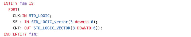
In this code snippet we have defined:
- The clock signal CLK input which is defined by the command “in std_logic”
- A 4-bit output port called CNT using “out std_logic_vector(3 downto 0)”
- A 4-bit input port called SEL using “in std_logic_vector(3 downto 0)”
Process and Data Type Defintions
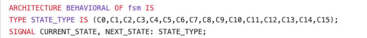
Now that we have defined the fsm entity, we can create an architecture for our circuit. This architecture will have three processes:
- The state memory.
- The next state logic.
- The output logic.
Before we can create these processes, we need to define a new data type for our states and two signal variables of that data type for memorizing the current and next states (think of them as registers).
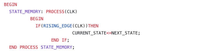
The State Memory Process
Now we can create our first process called STATE_MEMORY. Using a IF statement, it writes the value of the next state into the current state variable on every rising edge of the CLK signal.
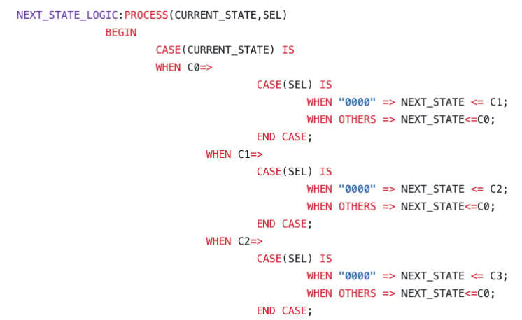
The Next State Logic Process
We’re going to create a process called NEXT_STATE_LOGIC using the SEL input port and the CURRENT_STATE signal. Inside this process, we call one CASE-WHEN statement for the current state. We nest additional CASE-WHEN statements for the mode inside of each WHEN clause of the first CASE-WHEN statement.
This way, we have an architecture that first checks the current state of the FSM and then reads the value from the SEL port. When this process finishes, the last nested WHEN clause will write the correct next state value to the NEXT_STATE signal according to our code (to the sequence being counted.)
The code chunk below shows a simple up counter that is active when the SEL port value is equal to “0000”. For brevity here, I am only showing a few of these repeating case statements, but the full code is provided further below.
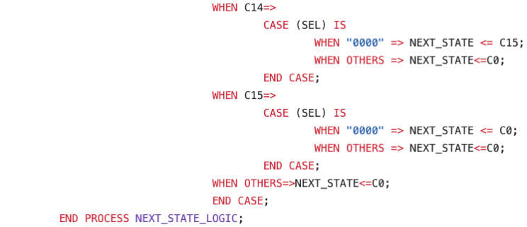
Skipping cases, C3 through C13 which are similar, we get to the end of the NEXT_STATE_LOGIC process where we have:
The Output Logic Process
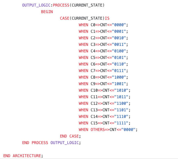
Lastly, in order for the current state to be output on the 4-bit LED display, we need to write another process called OUTPUT_LOGIC. It enumerates each state type we defined earlier with a corresponding 4-bit binary number.
This is again done by using the CURRENT_STATE signal and calling another CASE-WHEN statement. The CNT output represents the current state as its 4-bit binary counterpart:
Uploading to the Development Board
Next, we need to compile the code once again before we can finally upload it to the development board. This process is carried out using a USB Blaster connected to the Altera MAX II via JTAG as shown in Figure 1.
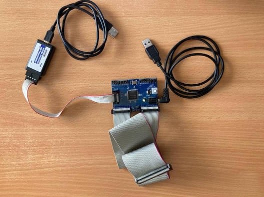
Figure 1. Altera board and USB Blaster connections. Image used courtesy of Kristijan Nelkovski
Adding an External Trigger
After uploading our code to the Altera board, we need to add a clock signal—some type of external trigger that allows our counter to iterate through its states. Here, I’m going to cheat a little bit and use a Raspberry Pi Pico running the default Arduino Blink sketch, which acts as a crude clock source for our circuit.
You can use any other MCU development board for this functionality; just ensure you send a 3.3 V logic-level signal to your Altera MAX II. The Raspberry Pi Pico natively outputs a 3.3 V logic signal.
In our circuit, the Blink sketch will provide a 0.5 Hz clock signal (you can change the frequency in the delay portion of the Arduino code). Instead of flashing an LED on for one second and then off for another second, it would tell our synchronous circuit when it’s time to switch to its next state, as defined in our VHDL code.
PCB Circuit Diagram
The schematic in Figure 2 shows the full circuit diagram of our project. Here, every LED is connected to an output pin through a current-limiting resistor, and every contact from the DIP switch that’s connected to an input pin is pulled down to ground using a resistor network. The clock pin is then connected to the supposed LED pin from the microcontroller board running Blink.
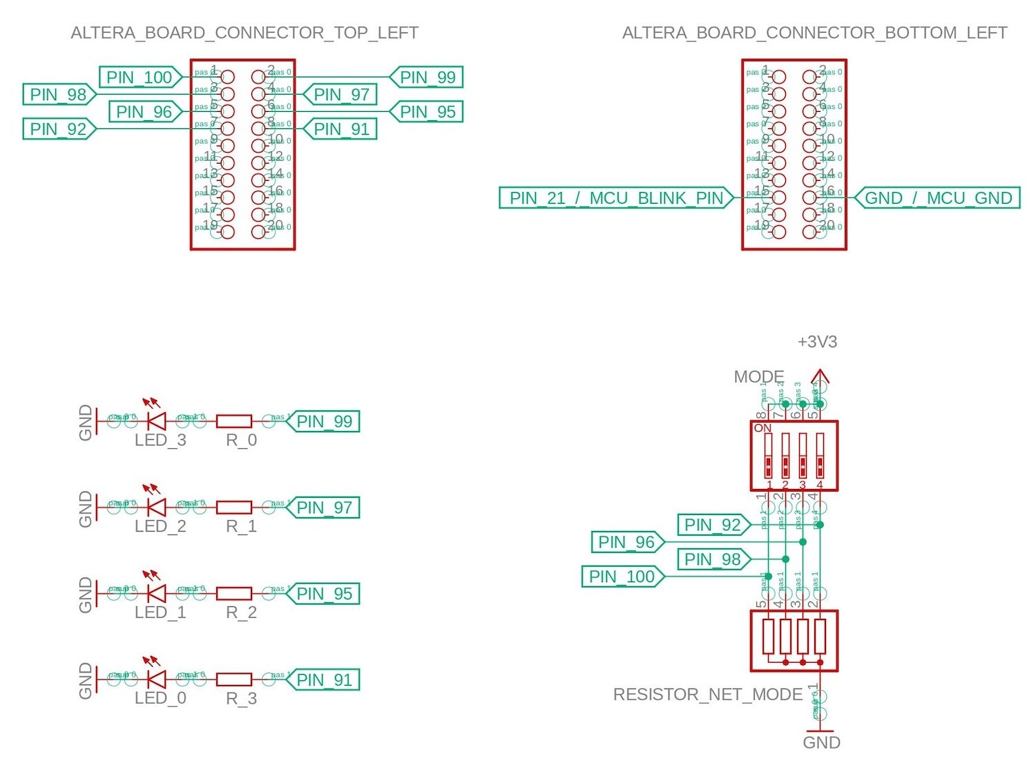
Figure 2. Circuit schematic of the 4-bit binary counter project. Image used courtesy of Kristijan Nelkovski
After wiring everything up and providing adequate power to the circuit, our FSM counter should start iterating through different binary sequences on its four LEDs according to the mode of counting selected through the DIP switch.
Designing Other Count Sequences
For other values of the SEL input you can create any arbitrary 4-bit number sequence. Inside the full code download at the end of this article, I’ve included 16 counting modes that can be selected using the 4-bit SEL input as described in Table 2.
Your Turn!
In this project, we created a finite-state machine circuit using the VHDL hardware description language and ran it on a CPLD development board. My goal with this series was to introduce programmable logic and give insights into the practical use of FPGA components using real hardware instead of circuit diagrams and computer simulations.
If you replicate this project, you can always play around with the code and switch up the counting modes or add and remove different sequences as you desire. Share your ideas and modifications in the comments below!
From https://www.bettlink.com/blog/from-vhdl-code-to-real-hardware--designing-a-finite-state-machine
LIBRARY IEEE; USE IEEE.STD_LOGIC_1164.ALL; ENTITY fsm IS PORT( CLK:IN STD_LOGIC; SEL: IN STD_LOGIC_vector(3 downto 0); CNT: OUT STD_LOGIC_VECTOR(3 DOWNTO 0)); END ENTITY fsm; ARCHITECTURE BEHAVIORAL OF fsm IS TYPE STATE_TYPE IS (C0,C1,C2,C3,C4,C5,C6,C7,C8,C9,C10,C11,C12,C13,C14,C15); SIGNAL CURRENT_STATE, NEXT_STATE: STATE_TYPE; BEGIN STATE_MEMORY: PROCESS(CLK) BEGIN IF(RISING_EDGE(CLK))THEN CURRENT_STATE<=NEXT_STATE; END IF; END PROCESS STATE_MEMORY; NEXT_STATE_LOGIC:PROCESS(CURRENT_STATE,SEL) BEGIN CASE(CURRENT_STATE) IS WHEN C0=> CASE(SEL) IS WHEN "0000" => NEXT_STATE <= C1; WHEN OTHERS => NEXT_STATE<=C0; END CASE; WHEN C1=> CASE(SEL) IS WHEN "0000" => NEXT_STATE <= C2; WHEN OTHERS => NEXT_STATE<=C0; END CASE; WHEN C2=> CASE(SEL) IS WHEN "0000" => NEXT_STATE <= C3; WHEN OTHERS => NEXT_STATE<=C0; END CASE; WHEN C3=> CASE(SEL) IS WHEN "0000" => NEXT_STATE <= C4; WHEN OTHERS => NEXT_STATE<=C0; END CASE; WHEN C4=> CASE(SEL) IS WHEN "0000" => NEXT_STATE <= C5; WHEN OTHERS => NEXT_STATE<=C0; END CASE; WHEN C5=> CASE(SEL) IS WHEN "0000" => NEXT_STATE <= C6; WHEN OTHERS => NEXT_STATE<=C0; END CASE; WHEN C6=> CASE(SEL) IS WHEN "0000" => NEXT_STATE <= C7; WHEN OTHERS => NEXT_STATE<=C0; END CASE; WHEN C7=> CASE(SEL) IS WHEN "0000" => NEXT_STATE <= C8; WHEN OTHERS => NEXT_STATE<=C0; END CASE; WHEN C8=> CASE(SEL) IS WHEN "0000" => NEXT_STATE <= C9; WHEN OTHERS => NEXT_STATE<=C0; END CASE; WHEN C9=> CASE (SEL) IS WHEN "0000" => NEXT_STATE <= C10; WHEN OTHERS => NEXT_STATE<=C0; END CASE; WHEN C10=> CASE (SEL) IS WHEN "0000" => NEXT_STATE <= C11; WHEN OTHERS => NEXT_STATE<=C0; END CASE; WHEN C11=> CASE (SEL) IS WHEN "0000" => NEXT_STATE <= C12; WHEN OTHERS => NEXT_STATE<=C0; END CASE; WHEN C12=> CASE (SEL) IS WHEN "0000" => NEXT_STATE <= C13; WHEN OTHERS => NEXT_STATE<=C0; END CASE; WHEN C13=> CASE (SEL) IS WHEN "0000" => NEXT_STATE <= C14; WHEN OTHERS => NEXT_STATE<=C0; END CASE; WHEN C14=> CASE (SEL) IS WHEN "0000" => NEXT_STATE <= C15; WHEN OTHERS => NEXT_STATE<=C0; END CASE; WHEN C15=> CASE (SEL) IS WHEN "0000" => NEXT_STATE <= C0; WHEN OTHERS => NEXT_STATE<=C0; END CASE; WHEN OTHERS=>NEXT_STATE<=C0; END CASE; END PROCESS NEXT_STATE_LOGIC; OUTPUT_LOGIC:PROCESS(CURRENT_STATE) BEGIN CASE(CURRENT_STATE)IS WHEN C0=>CNT<="0000"; WHEN C1=>CNT<="0001"; WHEN C2=>CNT<="0010"; WHEN C3=>CNT<="0011"; WHEN C4=>CNT<="0100"; WHEN C5=>CNT<="0101"; WHEN C6=>CNT<="0110"; WHEN C7=>CNT<="0111"; WHEN C8=>CNT<="1000"; WHEN C9=>CNT<="1001"; WHEN C10=>CNT<="1010"; WHEN C11=>CNT<="1011"; WHEN C12=>CNT<="1100"; WHEN C13=>CNT<="1101"; WHEN C14=>CNT<="1110"; WHEN C15=>CNT<="1111"; WHEN OTHERS=>CNT<="0000"; END CASE; END PROCESS OUTPUT_LOGIC; END ARCHITECTURE;
From VHDL Code to Real Hardware: Designing a Finite-State Machine


Raspberry Pi 5 7 Inch Touch Screen IPS 1024x600 HD LCD HDMI-compatible Display for RPI 4B 3B+ OPI 5 AIDA64 PC Secondary Screen(Without Speaker)
BUY NOW
ESP32-S3 4.3inch Capacitive Touch Display Development Board, 800×480, 5-point Touch, 32-bit LX7 Dual-core Processor
BUY NOW
Raspberry Pi 5 7 Inch Touch Screen IPS 1024x600 HD LCD HDMI-compatible Display for RPI 4B 3B+ OPI 5 AIDA64 PC Secondary Screen(Without Speaker)
BUY NOW
- Comments(1)
- Likes(0)
 Log in to post comments.
 Reply
Reply
 More by sky Lin
-
Commodore 64 1541-II Floppy Disk Drive C64 Power Supply Unit USB-C 5V 12V DIN connector 5.25
133 1 2 -
Easy to print simple stacking organizer with drawers
76 0 0 -
-
-
Modifying a Hotplate to a Reflow Solder Station
1117 1 6 -
MPL3115A2 Barometric Pressure, Altitude, and Temperature Sensor
628 0 1 -
-
-
V2 Commodore AMIGA USB-C Power Sink Delivery High Efficiency Supply Triple Output 5V ±12V OLED display ATARI compatible shark 100W
1402 4 3