I made 200Watt Class D amplifier
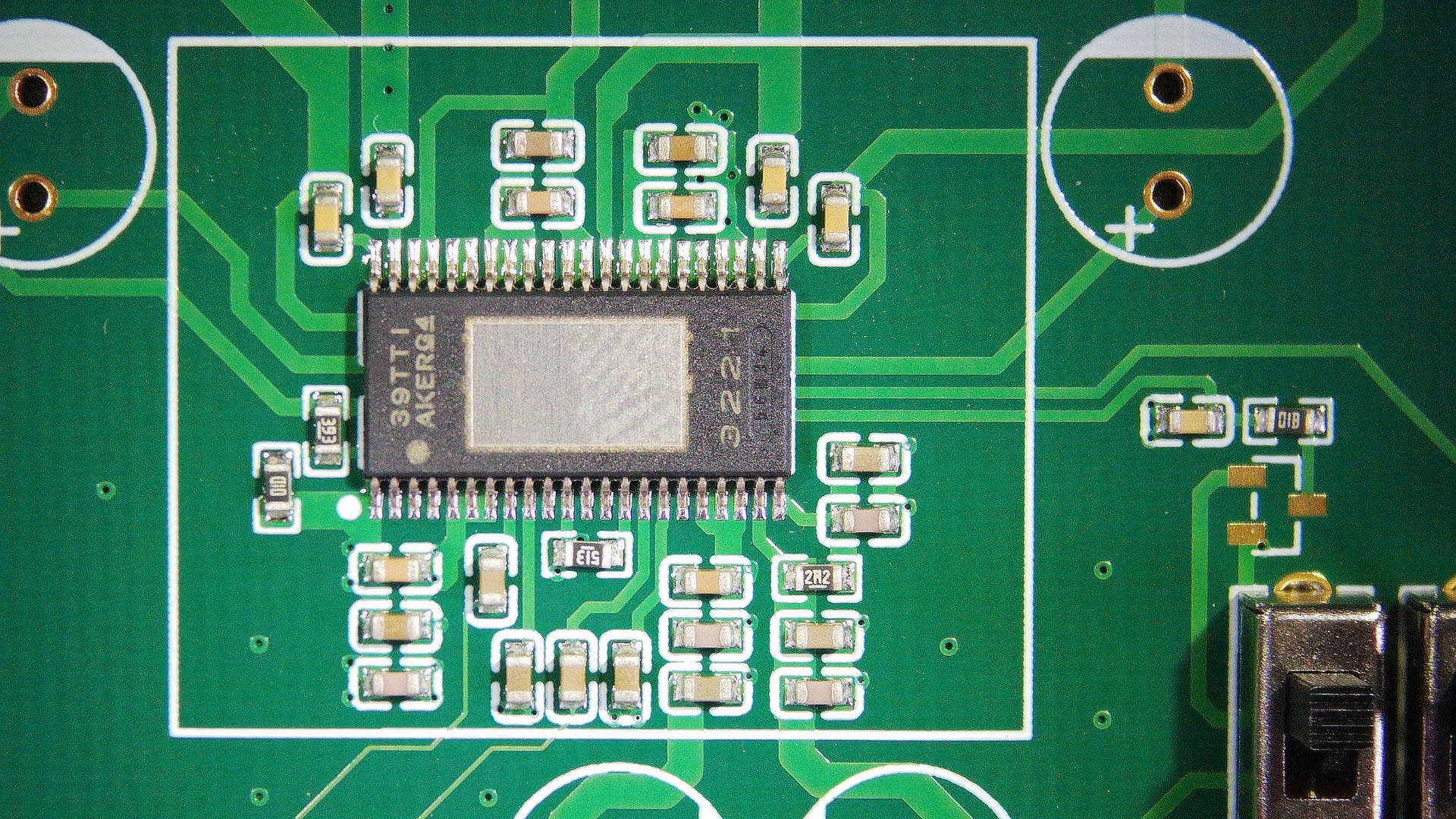
I have designed this 200W Class D amplifier board, which is separated into 100+100 Watt stereo channels. I went for TPA3221 for its great features, listed below. Moreover this audio amplifier can be used with bookshelf speakers and in home theater systems. The amplifier is capable of generating 170W power at 1% total harmonic distortion with 2 ohm speaker load in PBTL configuration. The board has selectable gains which can be altered by using different resistors settings, but for this design I adopted a max gain of 30dB.
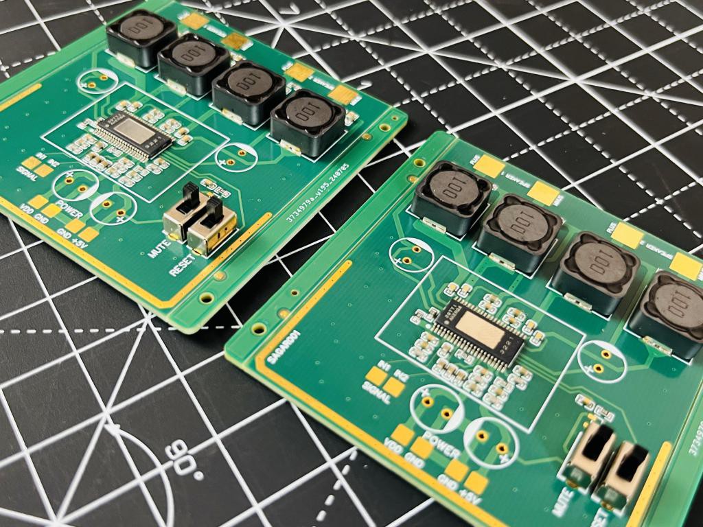
The amplifier can be supplied with a 7-30V power supply, but I will recommend using at least 24V 10A SMPS with this. The best feature of Class D amplifiers I have found is low heat dissipation, high efficiency and these amplifiers do not need dual rail power supplies, so the power supply section is easy to design. This project is sponsored by PCBWAY, China based PCB manufacturer having 10 years of experience in working with PCB related products. PCBWAY is a one stop solution to all your prototyping requirements including SMT assembly, Stencil, 3d printing and metal CNC.
Features of TPA3221 IC:
- Wide 7-V to 30-V Supply Voltage Operation
- Stereo (2 x BTL) and Mono (1 x PBTL) Operation Low-Power Operating Modes
- Standby Modes: Mute and < 1 mA Shutdown, Low Idle-Current HEAD Modulation
- Multiple Input Options to Simplify Preamp Design
- Differential or Single-Ended Analog Inputs
- Selectable Gains: 18 dB, 24 dB, 30 dB, 34 dB
- Integrated Protection: Undervoltage, Overvoltage,Short Circuit, Clipping Detection, Over Temperature Warning and Shutdown.
- Inbuilt DC Speaker Protection
- 90% Efficient Class-D Operation (4 Ω)
Circuit Diagram:
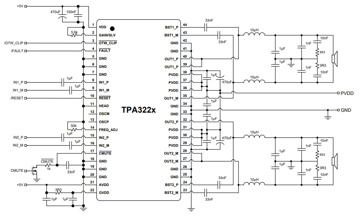
I have taken the reference directly from the TI datasheet, usually TI engineers post an application circuit with calculated values at the end of the datasheet with PCB layout design. In this way anyone with good electronics skill can design the circuit by following the notes and precautions. For some features we have to read the entire datasheet and sometimes may have to calculate the values as per desired response. So I modified the circuit according to my design specifications. And the finalized circuit is attached below.
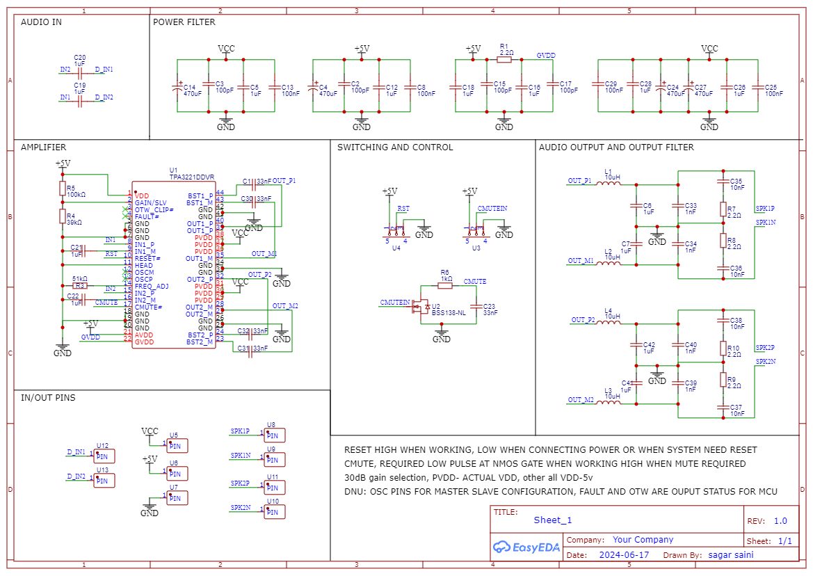
The updated schematics is divided into different sections as per usage, Power filters to decay down power supply input noises. Then the main amplifier which contains all the main gain and mode settings. Then reset and mute section, to avoid power on noise we have to turn off reset button after powering. To mute the device when it is operating at full potential mute switch can be turned on. Then the main output section contains signal filters, which turn the Class D PWM signal into analog output. And the final section contains I/O pins.
PCB Design:
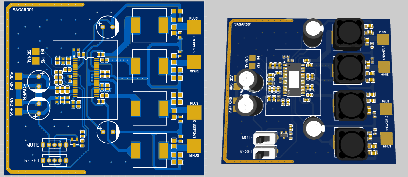
The board is designed on a 4 Layer PCB stackup to minimize the noise and any humming in the circuit ground plane is used underneath the main signal layer. The proper stackup of the PCB is defined as Signal/GND/5V/Signal. The output section is routed away from the input section so that any backpropagation and signal crossover do not happen in the PCB. As per datasheet the decoupling capacitors are used near to main IC, near to power pins so any noise in the input power supply signal can be eliminated. I used the PCBWAY SMT assembly process to get the soldering and part placement done easily.
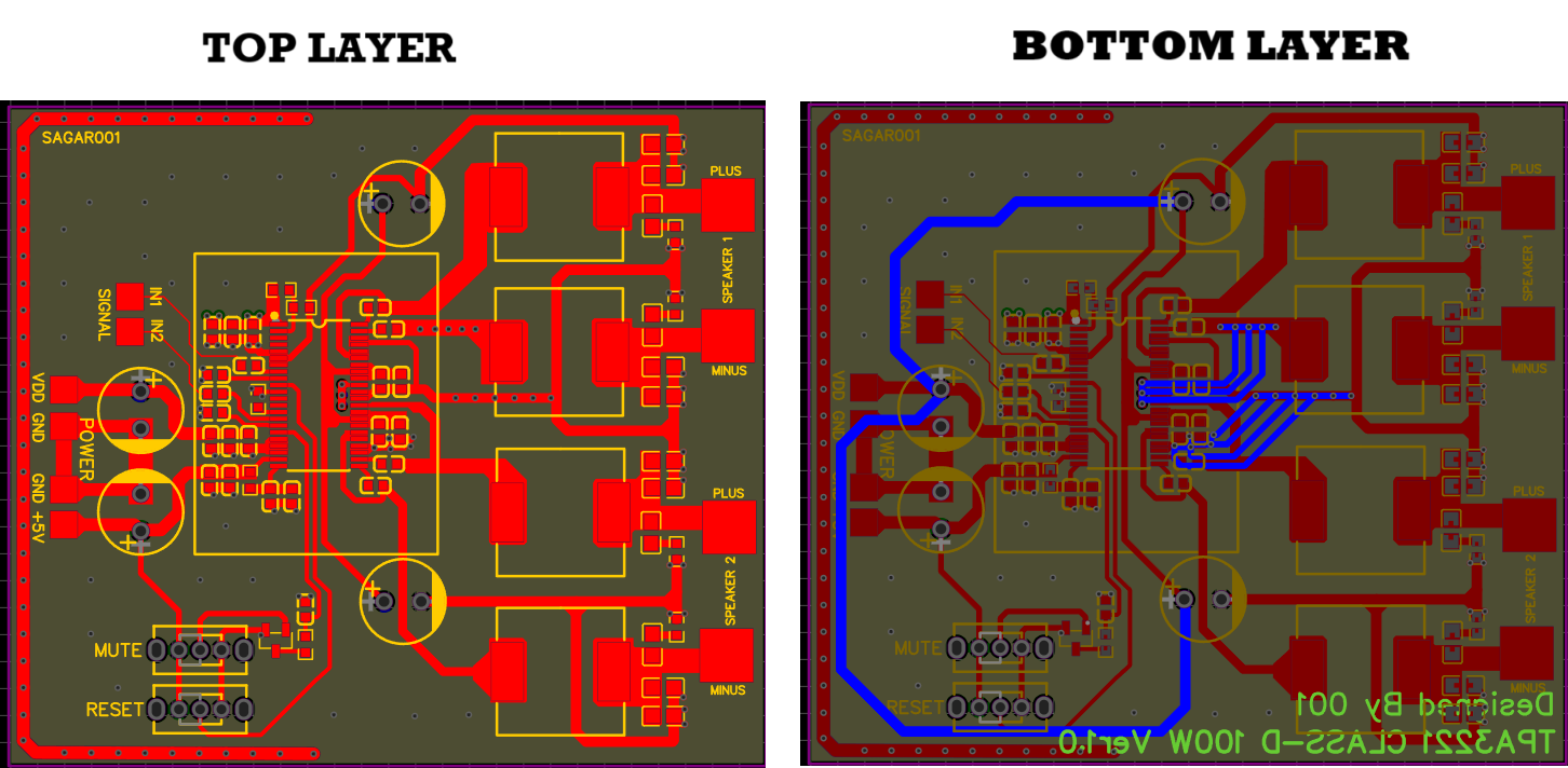
To route the main input audio signal 50 ohm line is used on the signal layer and to route the output section polygon planes are used. Vias at different points in signal and power planes are avoided to reduce the noise. The best practice to route the output section with via’s is to use different via’s with the same track in this way the current is distributed in the different tracks and propagation of signal is possible easily. I have stitched the signal layer copper pour with the ground plane to reduce the EMI problems in the circuit. Download all the design files from here.
Connection and Power ON:
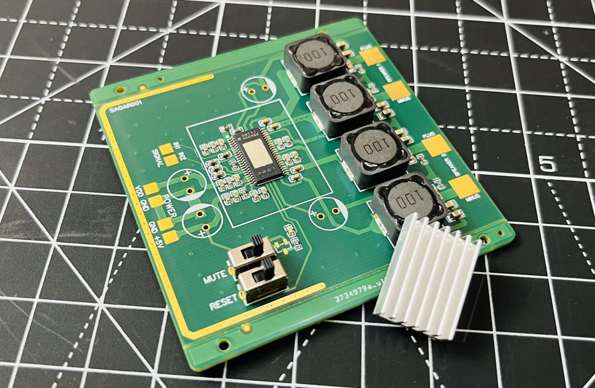
Two slide switches can be seen on the top layer of the board. One is to reset the IC, and one is used as a mute switch. Reset can be turned off after powering the IC, in this way any glitches in the output can be eliminated. CMute switches are connected to a MOSFET which is controlling the Mute pin of the IC, this is used to power off the amplifier from active output mode.
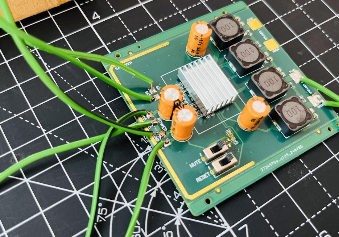
For the power input, two different isolated supplies can be externally connected to the amplifier. One to provide the logic 5 volt signal to the amplifier to turn on the logic function of the amplifier and a 30V supply as the main power supply unit, ground will remain the common for both.
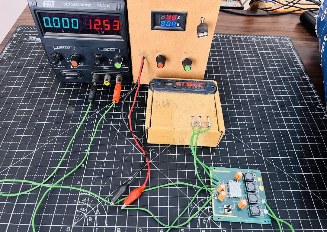
For audio input signals from any audio source like bluetooth, Mobile/Laptop Aux or from DSP can be given to the amplifier. A max of 5v peak to peak can be fed for the maximum signal output. I will recommend using a preamplifier which also opens up the options of frequency controlling like bass and treble.
Working and Testing:
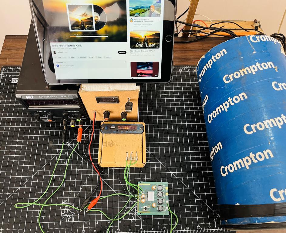
Here I have attached a video, here you can see the raw audio performance. The testing setup includes a DSP unit, 24V 10A power supply and 200W subwoofer. Test at 70% volume the amplifier performs best and produces very low heat which can be dissipated by a 40x30mm passive heat sink.
Final words:
The audio performance of the amplifier is quite good, not having any problems of noise or hum at the power ON. The filter section is well designed to convert the PWM to analog audio signal. Overall the amplifier performs well, as tested out with the custom made DSP and preamplifier unit. The highs, mid and low bass frequency is clear as used with the tweeter, subwoofer and woofer. Some distortion in the voice clarity can be seen at max volume output of the amplifier in the medium frequency range. Try the best PCB services now and turn your dream projects into real world applications with PCBWAY.
I made 200Watt Class D amplifier
*PCBWay community is a sharing platform. We are not responsible for any design issues and parameter issues (board thickness, surface finish, etc.) you choose.
- Comments(1)
- Likes(4)
-
 ANDRII
Nov 12,2025
-
 Satvir
Jun 25,2025
-
 Prasanna K
Sep 28,2024
-
 Josue Fernandez
Sep 25,2024
- 0 USER VOTES
- YOUR VOTE 0.00 0.00
- 1
- 2
- 3
- 4
- 5
- 6
- 7
- 8
- 9
- 10
- 1
- 2
- 3
- 4
- 5
- 6
- 7
- 8
- 9
- 10
- 1
- 2
- 3
- 4
- 5
- 6
- 7
- 8
- 9
- 10
- 1
- 2
- 3
- 4
- 5
- 6
- 7
- 8
- 9
- 10
 More by Engineer
-
 DIY a Smart NiMH/NiCd Battery Charger
When talking about standalone single cell battery chargers only one popular name came into my mind t...
-
 LiFePO4 Battery Charger With Protection
In the previous few months I tried to cover almost all types of battery charging integrated circuits...
-
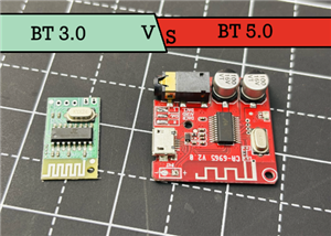 Comparison of Audio Bluetooth 3.0 and 5.0
Coming to bluetooth in audio applications, we have versions from 3.0 to 5.4. In the practical audio ...
-
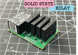 4 Channel SOLID STATE RELAY Module
I have designed a triac and optocoupler based project in the past, in which triac act as a relay and...
-
 A Look at Capacitive Water Overflow Sensor
Detection of Water overflow in a tank is one of the main topics when it comes to energy saving appli...
-
 Offline Voice Recognition Hub Based on ESPNOW
An offline voice recognition hub, no internet connection, no wifi router. Just a pair of ESP8266 wit...
-
 DIY a 200W Precise Electronic Load
Whenever I want to test some USB power supplies, drawing I-V characters of a power supply and workin...
-
 Smallest 220V to 5V Supply for IOT applications
The requirement of stable DC power supplies in the IOT applications and in electronics designed prod...
-
 I made 200Watt Class D amplifier
I have designed this 200W Class D amplifier board, which is separated into 100+100 Watt stereo chann...
-
 iPAD Pencil Backup Pocket Charger
I have a clone iPAD pencil which works in the similar way of Apple pencil, but this one comes with C...
-
 Digital Radio Transmitter and Receiver 433Mhz
Radio technology is the best monitoring and control solution for small and long range wireless hobby...
-
-
mammoth-3D SLM Voron Toolhead – Manual Drill & Tap Edition
232 0 0 -
-
AEL-2011 Power Supply Module
757 0 2 -
AEL-2011 50W Power Amplifier
632 0 2 -
-
-
Custom Mechanical Keyboard
825 0 0 -
Tester for Touch Screen Digitizer without using microcontroller
450 2 2 -
Audio reactive glow LED wristband/bracelet with NFC / RFID-Tags
402 0 1 -
-


