SMART HOME AUTOMATION
Schematic Design: Create a detailed schematic diagram illustrating the connections between the ESP microcontroller, sensors, relays, and other components.
PCB Layout: Design the PCB layout using a tool like EasyEDA or KiCad, ensuring proper trace routing and component placement for optimal performance.
Prototyping: Build a prototype of the PCB to test the functionality and identify any issues.
PCB Manufacturing: Use a reliable PCB manufacturing service, such as PCBWay, to produce the final PCB based on your design.
Assembly: Assemble the components onto the PCB, adhering to the layout and schematic.
Testing: Rigorously test the assembled PCB to ensure all components operate as intended.
Enclosure Design: If necessary, design an enclosure to house the PCB, providing protection and aesthetics.
Integration: Connect the smart home automation system to various devices and configure the mobile app for seamless remote control.
SMART HOME AUTOMATION
*PCBWay community is a sharing platform. We are not responsible for any design issues and parameter issues (board thickness, surface finish, etc.) you choose.


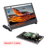
Raspberry Pi 5 7 Inch Touch Screen IPS 1024x600 HD LCD HDMI-compatible Display for RPI 4B 3B+ OPI 5 AIDA64 PC Secondary Screen(Without Speaker)
BUY NOW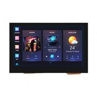
ESP32-S3 4.3inch Capacitive Touch Display Development Board, 800×480, 5-point Touch, 32-bit LX7 Dual-core Processor
BUY NOW
Raspberry Pi 5 7 Inch Touch Screen IPS 1024x600 HD LCD HDMI-compatible Display for RPI 4B 3B+ OPI 5 AIDA64 PC Secondary Screen(Without Speaker)
BUY NOW
- Comments(0)
- Likes(0)
 Log in to post comments.
More by PALANI MURUGAN L
-
-
Commodore 64 1541-II 1581 Floppy Disk Drive C64 Power Supply Unit USB-C 5V 12V DIN connector 5.25
280 1 3 -
Easy to print simple stacking organizer with drawers
106 0 0 -
-
-
-
-
-
Modifying a Hotplate to a Reflow Solder Station
1195 1 6 -
MPL3115A2 Barometric Pressure, Altitude, and Temperature Sensor
680 0 1 -