Ali Vural
TURKEY • + Follow
Edit Project
Description
JB Design for Antennas
The JB PCB I've designed facilitates the insertion of cables into an antenna's slot and enables their soldering.
The Live Line and Shields are intentionally short-circuited to serve the purpose of Junction Box.
Schematic and Layout

Dec 18,2023
380 views
end-flag
JB Design for Antennas
Designed a JB PCB: fits into antenna slot, allows cable soldering. Live end and shields intentionally short-circuited for JB purpose
380
0
0
Published: Dec 18,2023
Download Gerber file 0
Purchase
Donation Received ($)
PCBWay Donate 10% cost To Author
*PCBWay community is a sharing platform. We are not responsible for any design issues and parameter issues (board thickness, surface finish, etc.) you choose.
Copy this HTML into your page to embed a link to order this shared project
Copy
Under the
Attribution-ShareAlike (CC BY-SA)
License.

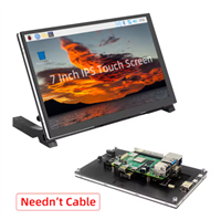
Raspberry Pi 5 7 Inch Touch Screen IPS 1024x600 HD LCD HDMI-compatible Display for RPI 4B 3B+ OPI 5 AIDA64 PC Secondary Screen(Without Speaker)
BUY NOW
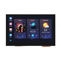
ESP32-S3 4.3inch Capacitive Touch Display Development Board, 800×480, 5-point Touch, 32-bit LX7 Dual-core Processor
BUY NOW
Raspberry Pi 5 7 Inch Touch Screen IPS 1024x600 HD LCD HDMI-compatible Display for RPI 4B 3B+ OPI 5 AIDA64 PC Secondary Screen(Without Speaker)
BUY NOW- Comments(0)
- Likes(0)
 Log in to post comments.
Upload photo
0 / 10000
It looks like you have not written anything. Please add a comment and try again.
You can upload up to 5 images!
Image size should not exceed 2MB!
File format not supported!
View More
VOTING
0 votes
- 0 USER VOTES
0.00
- YOUR VOTE 0.00 0.00
- 1
- 2
- 3
- 4
- 5
- 6
- 7
- 8
- 9
- 10
Design
1/4
- 1
- 2
- 3
- 4
- 5
- 6
- 7
- 8
- 9
- 10
Usability
2/4
- 1
- 2
- 3
- 4
- 5
- 6
- 7
- 8
- 9
- 10
Creativity
3/4
- 1
- 2
- 3
- 4
- 5
- 6
- 7
- 8
- 9
- 10
Content
4/4
 More by Ali Vural
You may also like
-
-
-
Modifying a Hotplate to a Reflow Solder Station
854 1 5 -
MPL3115A2 Barometric Pressure, Altitude, and Temperature Sensor
444 0 1 -
-
Nintendo 64DD Replacement Shell
376 0 2 -
V2 Commodore AMIGA USB-C Power Sink Delivery High Efficiency Supply Triple Output 5V ±12V OLED display ATARI compatible shark 100W
1093 4 2 -
How to measure weight with Load Cell and HX711
692 0 3


