|
TE AMP 1-1734530-1 female VGA connectorTE AMP
|
x 1 | |
|
|
68Ω ResistorJaycar Electronics
|
x 2 | |
|
|
470Ω ResistorJaycar Electronics
|
x 2 | |

|
MDJ-006-FSADAM TECH
|
x 1 |

|
fritzing |
VGA-AVR: An Arduino-Compatible VGA Shield for AVR Microcontrollers.
The VGA-AVR is an Arduino-compatible shield designed for outputting video to any monitor and receiving data from any keyboard with its onboard VGA connector and PS/2 6-pin Mini-DIN connector. The shield was designed originally for hobbyists who wanted to make something retro and useful with their Arduino, particularly those who wanted to replicate the technology of the 80s, such as the Apple II and the Commodore 64. It would be nice if anyone develops some software for this shield but it supports the 'vgax' and 'PS/2 Advanced' library for Arduino, which will be included below.
Enjoy, and continue hacking, Hackers!

VGA-AVR: An Arduino-Compatible VGA Shield for AVR Microcontrollers.
*PCBWay community is a sharing platform. We are not responsible for any design issues and parameter issues (board thickness, surface finish, etc.) you choose.

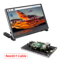
Raspberry Pi 5 7 Inch Touch Screen IPS 1024x600 HD LCD HDMI-compatible Display for RPI 4B 3B+ OPI 5 AIDA64 PC Secondary Screen(Without Speaker)
BUY NOW
ESP32-S3 4.3inch Capacitive Touch Display Development Board, 800×480, 5-point Touch, 32-bit LX7 Dual-core Processor
BUY NOW
Raspberry Pi 5 7 Inch Touch Screen IPS 1024x600 HD LCD HDMI-compatible Display for RPI 4B 3B+ OPI 5 AIDA64 PC Secondary Screen(Without Speaker)
BUY NOW- Comments(10)
- Likes(0)
- 0 USER VOTES
- YOUR VOTE 0.00 0.00
- 1
- 2
- 3
- 4
- 5
- 6
- 7
- 8
- 9
- 10
- 1
- 2
- 3
- 4
- 5
- 6
- 7
- 8
- 9
- 10
- 1
- 2
- 3
- 4
- 5
- 6
- 7
- 8
- 9
- 10
- 1
- 2
- 3
- 4
- 5
- 6
- 7
- 8
- 9
- 10
 More by Sudo Net
-
-
-
-
Modifying a Hotplate to a Reflow Solder Station
999 1 6 -
MPL3115A2 Barometric Pressure, Altitude, and Temperature Sensor
543 0 1 -
-
Nintendo 64DD Replacement Shell
443 0 2 -
V2 Commodore AMIGA USB-C Power Sink Delivery High Efficiency Supply Triple Output 5V ±12V OLED display ATARI compatible shark 100W
1269 4 2 -
How to measure weight with Load Cell and HX711
760 0 3


Oh, yes! Thank you for noticing that! I will fix it IMMEDIATELY! Damn, it sure is a disaster!
All fixed! Thanks for your quick reply!
There are still many DFM errors in the latest gerber, please check again.
Decided to place the traces on different layers. I hope this helps, considering this is supposed to be a 2-layer pcb.
Sharp angles and right angles should be avoided in PCB design, otherwise, unnecessary radiation will be generated and the process performance will be poor. https://www.pcbway.com/helpcenter/design_instruction/Common_Rules_for_PCB_Routing.html
Alright. I am currently chamfering them. Don't worry.
All chamfering is now done!
Hello! It is now fixed!