Dale
AUSTRALIA • + Follow
Edit Project

Description
Z80 LED Breakout Board UNTESTED!
Z80 LED Breakout Board for Mike @'vintage {Computers | Microprocessors | Microcontrollers}'
Mar 17,2019
1,676 views
end-flag
Z80 LED Breakout Board UNTESTED!
2 Layers PCB 100 x 100 mm FR-4, 1.6 mm, 1, HASL with lead, Green Solder Mask, White silkscreen
1676
4
1
6.50 (1)
Published: Mar 17,2019
Download Gerber file 14
Purchase
Donation Received ($)
PCBWay Donate 10% cost To Author
*PCBWay community is a sharing platform. We are not responsible for any design issues and parameter issues (board thickness, surface finish, etc.) you choose.
Copy this HTML into your page to embed a link to order this shared project
Copy
Under the
Attribution-ShareAlike (CC BY-SA)
License.

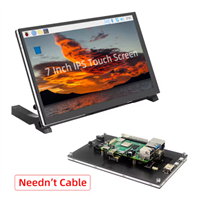
Raspberry Pi 5 7 Inch Touch Screen IPS 1024x600 HD LCD HDMI-compatible Display for RPI 4B 3B+ OPI 5 AIDA64 PC Secondary Screen(Without Speaker)
BUY NOW
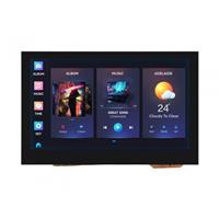
ESP32-S3 4.3inch Capacitive Touch Display Development Board, 800×480, 5-point Touch, 32-bit LX7 Dual-core Processor
BUY NOW
Raspberry Pi 5 7 Inch Touch Screen IPS 1024x600 HD LCD HDMI-compatible Display for RPI 4B 3B+ OPI 5 AIDA64 PC Secondary Screen(Without Speaker)
BUY NOW
Topic
- Comments(1)
- Likes(4)
 Log in to post comments.
Upload photo
0 / 10000
It looks like you have not written anything. Please add a comment and try again.
You can upload up to 5 images!
Image size should not exceed 2MB!
File format not supported!
 Paul Laba
 Apr 03,20210 CommentsReply
-
 (DIY) C64iSTANBUL
Jul 12,2022
-
 Arpad Attila Bakos
Jun 10,2021
-
 Bertote
Jun 09,2021
-
 ever
Dec 18,2020
View More
VOTING
1 votes
- 1 USER VOTES
6.50
- YOUR VOTE 0.00 0.00
- 1
- 2
- 3
- 4
- 5
- 6
- 7
- 8
- 9
- 10
Design
1/4
- 1
- 2
- 3
- 4
- 5
- 6
- 7
- 8
- 9
- 10
Usability
2/4
- 1
- 2
- 3
- 4
- 5
- 6
- 7
- 8
- 9
- 10
Creativity
3/4
- 1
- 2
- 3
- 4
- 5
- 6
- 7
- 8
- 9
- 10
Content
4/4
-
5design
-
5usability
-
7creativity
-
9content
6.50
 More by Dale
You may also like
-
-
-
Modifying a Hotplate to a Reflow Solder Station
689 1 5 -
MPL3115A2 Barometric Pressure, Altitude, and Temperature Sensor
370 0 1 -
-
Nintendo 64DD Replacement Shell
333 0 2 -
V2 Commodore AMIGA USB-C Power Sink Delivery High Efficiency Supply Triple Output 5V ±12V OLED display ATARI compatible shark 100W
901 4 2 -
How to measure weight with Load Cell and HX711
607 0 3


 Top%20Overlay
 Top%20Solder%20Mask
 Top%20Copper%20Layer
 Mechanical%20Layer%201
 Bottom%20Overlay
 Bottom%20Solder%20Mask
 Bottom%20Copper%20Layer
 Bottom
 Top
Top


