PCB Prototype the Easy Way
Full feature custom PCB prototype service.
9:00 - 18:00, Mon.- Fri. (GMT+8)
9:00 - 12:00, Sat. (GMT+8)
(Except Chinese public holidays)
PCB Prototype the Easy Way
Full feature custom PCB prototype service.
9:00 - 18:00, Mon.- Fri. (GMT+8)
9:00 - 12:00, Sat. (GMT+8)
(Except Chinese public holidays)
Reason of failed review:
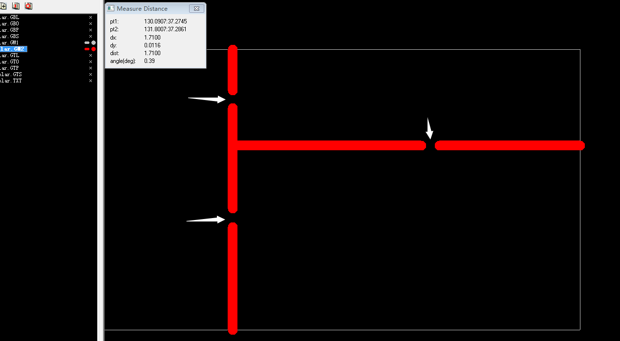
Per file, the boards are panelized by tab routing. But, we are unable to find stamp holes on tab routing.
Suggestion:
When you upload gerber file, if it is tab routing, please make sure the tab routing meets our capability of 1.6mm and add stamp holes. The minimum size of stamp hole is in 0.5-0.6mm and
spacing is over 0.25mm.

 Log in to post comments.