|
74HC595D,118NXP USA Inc.
|
x 8 | |

|
CFR-12JB-52-220RYAGEO
|
x 64 | |

|
2N2222ADiotec Semiconductor
|
x 16 | |

|
16 pin male header |
x 10 | |
|
|
Ic Base |
x 8 | |

|
Push Switch Tactile Momentary 12mm |
x 1 |

|
arduino IDEArduino
|
8*8*8 Led Cube Driver Pcb
Shift register
A shift register is a type of digital circuit using a cascade of flip-flops where the output of one flip-flop is connected to the input of the next. They share a single clock signal, which causes the data stored in the system to shift from one location to the next. By connecting the last flip-flop back to the first, the data can cycle within the shifters for extended periods, and in this form they were used as a form of computer memory. In this role they are very similar to the earlier delay-line memory systems and were widely used in the late 1960s and early 1970s to replace that form of memory.
In most cases, several parallel shift registers would be used to build a larger memory pool known as a "bit array". Data was stored into the array and read back out in parallel, often as a computer word, while each bit was stored serially in the shift registers. There is an inherent trade-off in the design of bit arrays; putting more flip-flops in a row allows a single shifter to store more bits, but requires more clock cycles to push the data through all of the shifters before the data can be read back out again.
Shift registers can have both parallel and serial inputs and outputs. These are often configured as "serial-in, parallel-out" (SIPO) or as "parallel-in, serial-out" (PISO). There are also types that have both serial and parallel input and types with serial and parallel output. There are also "bidirectional" shift registers, which allow shifting in both directions: L& nbsp;→& nbsp;R or R& nbsp;→& nbsp;L. The serial input and last output of a shift register can also be connected to create a "circular shift register". A PIPO register (parallel in, parallel out) is very fast – an output is given within a single clock pulse.
Serial-in serial-out (SISO)
Sample usage of a 4-bit shift register. Data input is 10110000.TimeOutput 1Output 2Output 3Output 4000001100020100310104110150110600117000180000
These are the simplest kind of shift registers. The data string is presented at "data in" and is shifted right one stage each time "data advance" is brought high. At each advance, the bit on the far left (i.e. "data in") is shifted into the first flip-flop's output. The bit on the far right (i.e. "data out") is shifted out and lost.
The data is stored after each flip-flop on the "Q" output, so there are four storage "slots" available in this arrangement, hence it is a 4-bit register. To give an idea of the shifting pattern, imagine that the register holds 0000 (so all storage slots are empty). As "data in" presents 1,0,1,1,0,0,0,0 (in that order, with a pulse at "data advance" each time—this is called clocking or strobing) to the register, this is the result. The right hand column corresponds to the right-most flip-flop's output pin, and so on.
So the serial output of the entire register is 00010110. It can be seen that if data were to be continued to input, it would get exactly what was put in (10110000), but offset by four "data advance" cycles. This arrangement is the hardware equivalent of a queue. Also, at any time, the whole register can be set to zero by bringing the reset (R) pins high.
This arrangement performs destructive readout – each datum is lost once it has been shifted out of the right-most bit.
Serial-in parallel-out (SIPO)

This configuration allows conversion from serial to parallel format. Data input is serial, as described in the SISO section above. Once the data has been clocked in, it may be either read off at each output simultaneously, or it can be shifted out.
In this configuration, each flip-flop is edge triggered. All flip-flops operate at the given clock frequency. Each input bit makes its way down to the Nth output after N clock cycles, leading to parallel output.
In cases where the parallel outputs should not change during the serial loading process, it is desirable to use a latched or buffered output. In a latched shift register (such as the 74595) the serial data is first loaded into an internal buffer register, then upon receipt of a load signal the state of the buffer register is copied into a set of output registers. In general, the practical application of the serial-in/parallel-out shift register is to convert data from serial format on a single wire to parallel format on multiple wires.
Parallel-in serial-out (PISO)
This configuration has the data input on lines D1 through D4 in parallel format, D1 being the most significant bit. To write the data to the register, the Write/Shift control line must be held LOW. To shift the data, the W/S control line is brought HIGH and the registers are clocked. The arrangement now acts as a PISO shift register, with D1 as the Data Input. However, as long as the number of clock cycles is not more than the length of the data-string, the Data Output, Q, will be the parallel data read off in order.
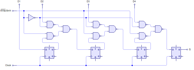
4-Bit PISO Shift Register
The animation below shows the write/shift sequence, including the internal state of the shift register.

Uses[edit]

Toshiba TC4015BP – dual 4-stage static shift register (with serial input/parallel output)
One of the most common uses of a shift register is to convert between serial and parallel interfaces. This is useful as many circuits work on groups of bits in parallel, but serial interfaces are simpler to construct. Shift registers can be used as simple delay circuits. Several bidirectional shift registers could also be connected in parallel for a hardware implementation of a stack.
SIPO registers are commonly attached to the output of microprocessors when more general-purpose input/output pins are required than are available. This allows several binary devices to be controlled using only two or three pins, but more slowly than by parallel output. The devices in question are attached to the parallel outputs of the shift register, and the desired state for all those devices can be sent out of the microprocessor using a single serial connection. Similarly, PISO configurations are commonly used to add more binary inputs to a microprocessor than are available – each binary input (such as a button or more complicated circuitry) is attached to a parallel input of the shift register, then the data is sent back via serial to the microprocessor using several fewer lines than originally required.
Shift registers can also be used as pulse extenders. Compared to monostable multivibrators, the timing has no dependency on component values, however, it requires external clock, and the timing accuracy is limited by a granularity of this clock. Example: Ronja Twister, where five 74164 shift registers create the core of the timing logic this way (schematic).
In early computers, shift registers were used to handle data processing: two numbers to be added were stored in two shift registers and clocked out into an arithmetic and logic unit (ALU) with the result being fed back to the input of one of the shift registers (the accumulator), which was one bit longer, since binary addition can only result in an answer that has the same size or is one bit longer.
Many computer languages include instructions to "shift right" and "shift left" the data in a register, effectively dividing by two or multiplying by two for each place shifted.
Very large serial-in serial-out shift registers (thousands of bits in size) were used in a similar manner to the earlier delay-line memory in some devices built in the early 1970s. Such memories were sometimes called "circulating memory". For example, the Datapoint 3300 terminal stored its display of 25 rows of 72 columns of 6-bit upper-case characters using 54 (arranged in 6 tracks of 9 packs) 200-bit shift registers, providing storage for 1800 characters. The shift register design meant that scrolling the terminal display could be accomplished by simply pausing the display output to skip one line of characters
When to use Shift Register?
Shift registers are often used for the purpose of saving pins on the microcontroller, as every microcontroller has a limited number of I/O pins (GPIO).
If your project needs to control 16 individual LEDs, that would normally require 16 pins of an Arduino. In the event that you don’t have 16 I/O pins available, this is where the shift register comes in handy. With two shift registers connected in series, we can accomplish the task of controlling the 16 LEDs with using only 3 I/O pins. And not just this; you can save even more pins the more shift registers you have chained together.
A real world example that uses shift register is the ‘Original Nintendo Controller’. The main controller of the Nintendo Entertainment System needed to get all button presses serially, and it used a shift register to accomplish that task.
Serial to Parallel Shifting-Out with a 74HC595
Shifting Out & the 595 chip
At sometime or another you may run out of pins on your Arduino board and need to extend it with shift registers. This example is based on the 74HC595. The datasheet refers to the 74HC595 as an "8-bit serial-in, serial or parallel-out shift register with output latches; 3-state." In other words, you can use it to control 8 outputs at a time while only taking up a few pins on your microcontroller. You can link multiple registers together to extend your output even more. (Users may also wish to search for other driver chips with "595" or "596" in their part numbers, there are many. The STP16C596 for example will drive 16 LED's and eliminates the series resistors with built-in constant current sources.)
How this all works is through something called "synchronous serial communication," i.e. you can pulse one pin up and down thereby communicating a data byte to the register bit by bit. It's by pulsing second pin, the clock pin, that you delineate between bits. This is in contrast to using the "asynchronous serial communication" of the Serial.begin() function which relies on the sender and the receiver to be set independently to an agreed upon specified data rate. Once the whole byte is transmitted to the register the HIGH or LOW messages held in each bit get parceled out to each of the individual output pins. This is the "parallel output" part, having all the pins do what you want them to do all at once.
The "serial output" part of this component comes from its extra pin which can pass the serial information received from the microcontroller out again unchanged. This means you can transmit 16 bits in a row (2 bytes) and the first 8 will flow through the first register into the second register and be expressed there. You can learn to do that from the second example.
"3 states" refers to the fact that you can set the output pins as either high, low or "high impedance." Unlike the HIGH and LOW states, you can"t set pins to their high impedance state individually. You can only set the whole chip together. This is a pretty specialized thing to do -- Think of an LED array that might need to be controlled by completely different microcontrollers depending on a specific mode setting built into your project. Neither example takes advantage of this feature and you won"t usually need to worry about getting a chip that has it.
Here is a table explaining the pin-outs adapted from the Phillip's datasheet.
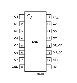
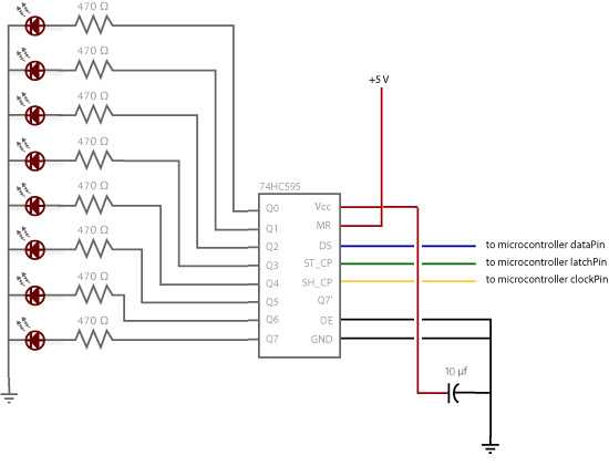
1. Turning it on
Make the following connections:
GND (pin 8) to ground,
Vcc (pin 16) to 5V
OE (pin 13) to ground
MR (pin 10) to 5V
This set up makes all of the output pins active and addressable all the time. The one flaw of this set up is that you end up with the lights turning on to their last state or something arbitrary every time you first power up the circuit before the program starts to run. You can get around this by controlling the MR and OE pins from your Arduino board too, but this way will work and leave you with more open pins.
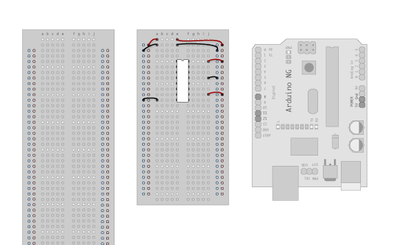
2. Connect to Arduino
DS (pin 14) to Ardunio DigitalPin 11 (blue wire)
SH_CP (pin 11) to to Ardunio DigitalPin 12 (yellow wire)
ST_CP (pin 12) to Ardunio DigitalPin 8 (green wire)
From now on those will be refered to as the dataPin, the clockPin and the latchPin respectively. Notice the 0.1"f capacitor on the latchPin, if you have some flicker when the latch pin pulses you can use a capacitor to even it out.
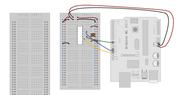
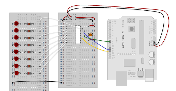
3. Add 8 LEDs.
In this case you should connect the cathode (short pin) of each LED to a common ground, and the anode (long pin) of each LED to its respective shift register output pin. Using the shift register to supply power like this is called sourcing current. Some shift registers can't source current, they can only do what is called sinking current. If you have one of those it means you will have to flip the direction of the LEDs, putting the anodes directly to power and the cathodes (ground pins) to the shift register outputs. You should check the your specific datasheet if you aren't using a 595 series chip. Don't forget to add a 470-ohm resistor in series to protect the LEDs from being overloaded.
Circuit Diagram
The Code
Here are three code examples. The first is just some "hello world" code that simply outputs a byte value from 0 to 255. The second program lights one LED at a time. The third cycles through an array.
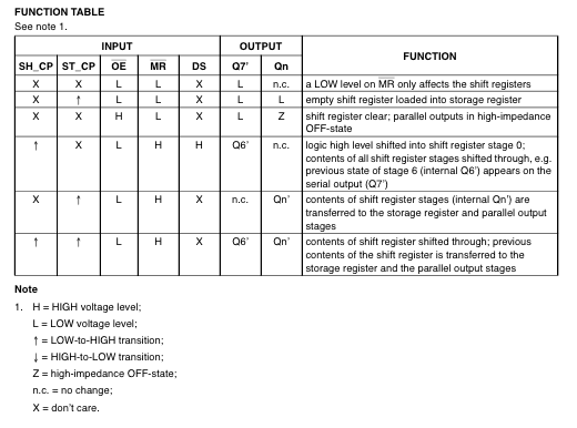
595 Logic Table
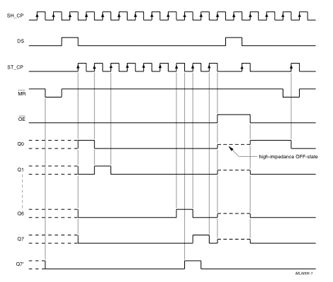
595 Timing Diagram
The code is based on two pieces of information in the datasheet: the timing diagram and the logic table. The logic table is what tells you that basically everything important happens on an up beat. When the clockPin goes from low to high, the shift register reads the state of the data pin. As the data gets shifted in it is saved in an internal memory register. When the latchPin goes from low to high the sent data gets moved from the shift registers aforementioned memory register into the output pins, lighting the LEDs.
Code Sample 1.1 Hello World Code Sample 1.2 One by One Code Sample 1.3 Using an array
Example 2
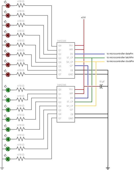
In this example you'll add a second shift register, doubling the number of output pins you have while still using the same number of pins from the Arduino.
The Circuit
1. Add a second shift register.
Starting from the previous example, you should put a second shift register on the board. It should have the same leads to power and ground.
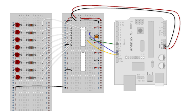
2. Connect the 2 registers.
Two of these connections simply extend the same clock and latch signal from the Arduino to the second shift register (yellow and green wires). The blue wire is going from the serial out pin (pin 9) of the first shift register to the serial data input (pin 14) of the second register.
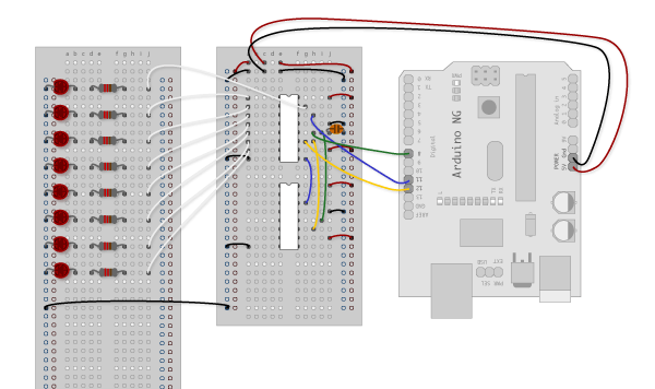
3. Add a second set of LEDs.
In this case I added green ones so when reading the code it is clear which byte is going to which set of LEDs
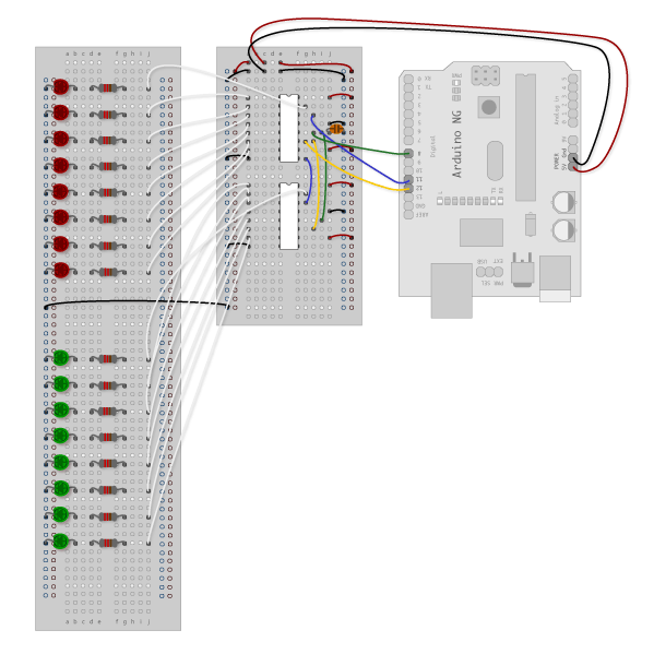
Circuit Diagram
The Code
Here again are three code samples. If you are curious, you might want to try the samples from the first example with this circuit set up just to see what happens.
Code Sample 2.1 Dual Binary Counters There is only one extra line of code compared to the first code sample from Example 1. It sends out a second byte. This forces the first shift register, the one directly attached to the Arduino, to pass the first byte sent through to the second register, lighting the green LEDs. The second byte will then show up on the red LEDs.
Code Sample 2.2 2 Byte One By One Comparing this code to the similar code from Example 1 you see that a little bit more has had to change. The blinkAll() function has been changed to the blinkAll_2Bytes() function to reflect the fact that now there are 16 LEDs to control. Also, in version 1 the pulsings of the latchPin were situated inside the subfunctions lightShiftPinA and lightShiftPinB(). Here they need to be moved back into the main loop to accommodate needing to run each subfunction twice in a row, once for the green LEDs and once for the red ones.
Code Sample 2.3 - Dual Defined Arrays Like sample 2.2, sample 2.3 also takes advantage of the new blinkAll_2bytes() function. 2.3's big difference from sample 1.3 is only that instead of just a single variable called "data" and a single array called "dataArray" you have to have a dataRED, a dataGREEN, dataArrayRED, dataArrayGREEN defined up front.
This means that line data = dataArray[j];
becomes
dataRED = dataArrayRED[j];
dataGREEN = dataArrayGREEN[j];
shiftOut(dataPin, clockPin, data);
becomes
shiftOut(dataPin, clockPin, dataGREEN);
shiftOut(dataPin, clockPin, dataRED);


8*8*8 Led Cube Driver Pcb
*PCBWay community is a sharing platform. We are not responsible for any design issues and parameter issues (board thickness, surface finish, etc.) you choose.
- Comments(0)
- Likes(2)
-
 Engineer
Jun 16,2022
-
 Darren Bassett
Jun 01,2022
- 0 USER VOTES
- YOUR VOTE 0.00 0.00
- 1
- 2
- 3
- 4
- 5
- 6
- 7
- 8
- 9
- 10
- 1
- 2
- 3
- 4
- 5
- 6
- 7
- 8
- 9
- 10
- 1
- 2
- 3
- 4
- 5
- 6
- 7
- 8
- 9
- 10
- 1
- 2
- 3
- 4
- 5
- 6
- 7
- 8
- 9
- 10
 More by Sreeram.zeno
-
 Esp12-F Cluster V1.0
The ESP8266 is a low-cost Wi-Fi microchip, with built-in TCP/IP networking software, and microcontro...
-
 TB6612FNG Motor Driver
The TB6612FNG Motor Driver can control up to two DC motors at a constant current of 1.2A (3.2A peak)...
-
 Sunny Buddy Solar Charger v1.0
This is the Sunny Buddy, a maximum power point tracking (MPPT) solar charger for single-cell LiPo ba...
-
 Diy 74HC4051 8 Channel Mux Breakout Pcb
The 74HC4051; 74HCT4051 is a single-pole octal-throw analog switch (SP8T) suitable for use in analog...
-
 Diy RFM97CW Breakout Pcb
IntroductionLoRa? (standing for Long Range) is a LPWAN technology, characterized by a long range ass...
-
 ProMicro-RP2040 Pcb
The RP2040 is a 32-bit dual ARM Cortex-M0+ microcontroller integrated circuit by Raspberry Pi Founda...
-
 Serial Basic CH340G Pcb
A USB adapter is a type of protocol converter that is used for converting USB data signals to and fr...
-
 Mp3 Shield For Arduino
Hardware OverviewThe centerpiece of the MP3 Player Shield is a VS1053B Audio Codec IC. The VS1053B i...
-
 MRK CAN Shield Arduino
The CAN-BUS Shield provides your Arduino or Redboard with CAN-BUS capabilities and allows you to hac...
-
 AVR ISP Programmer
AVR is a family of microcontrollers developed since 1996 by Atmel, acquired by Microchip Technology ...
-
 Diy Arduino mega Pcb
The Arduino Mega 2560 is a microcontroller board based on the ATmega2560. It has 54 digital input/ou...
-
 Max3232 Breakout Board
MAX3232 IC is extensively used for serial communication in between Microcontroller and a computer fo...
-
 Line Follower Pcb
The Line Follower Array is a long board consisting of eight IR sensors that have been configured to ...
-
 HMC6343 Accelerometer Module
The HMC6343 is a solid-state compass module with tilt compensation from Honeywell. The HMC6343 has t...
-
 RTK2 GPS Module For Arduino
USBThe USB C connector makes it easy to connect the ZED-F9P to u-center for configuration and quick ...
-
 Arduino Explora Pcb
The Arduino Esplora is a microcontroller board derived from the Arduino Leonardo. The Esplora differ...
-
 Diy Stepper Motor Easy Driver
A motor controller is a device or group of devices that can coordinate in a predetermined manner the...
-
 Diy Arduino Pro Mini
The Arduino Pro Mini is a microcontroller board based on the ATmega168 . It has 14 digital input/out...
-
TEKTRONIX THS710,THS720,THS730 External Battery Charger with 3D Printed Case
28 1 0 -
-
Atomic Force Microscope - electronic part
97 0 0 -


