As a new PCB designer, you may encounter many specialized terminologys related to printed circuit boards, which can often be confusing. Engineering courses typically focus more on system design and semiconductors rather than PCB design, so they offer limited help in this area. However, the circuit board is the crucial link between these fields, making it essential to master basic terminology.
To help new designers better understand printed circuit board terminology, we have compiled a list of common terminologys. By familiarizing yourself with these terminologys, you will be able to communicate more effectively with colleagues and gain a deeper understanding of the design and manufacturing process of printed electronics. We will introduce the terminology of printed circuit boards from the following three aspects:
Terminologys describing the physical structure of PCBs
Common terminologys used in PCB design
Terminologys related to manufacturing
PCB Physical Structure Terminologys
Some key printed circuit board terminologys are commonly used to describe the physical structure of PCBs, so understanding them is very important.
Layers: A circuit board is composed of multiple layers that are laminated together to form a single unit. Each layer has etched copper to create the conductive paths on each layer's surface.
Copper Pour: In a PCB, there are some areas filled with copper, and the shapes of these areas can vary.
Traces and transmission lines: These two terms can be used interchangeably in advanced high-speed PCB design, referring to the conductive paths.
Signal vs. plane layer: The signal layer is mainly used for transmitting electrical signals, but it can also contain copper areas for ground or power. The plane layer is used for distributing power or ground, and it is usually a complete copper plane.
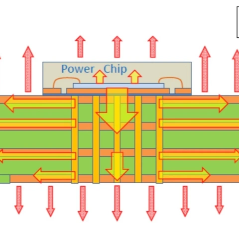
Vias: Vias are used to connect different layers of circuit boards, facilitating the transmission of electrical signals and power connections, and aiding in the realization of complex circuit layouts and designs. They can be through-hole vias, blind vias, or buried vias.
Components: Refers to any part placed on a PCB, including basic components like resistors, connectors, integrated circuits, and more. Components can be mounted by being soldered to the surface (SMD components) or by having leads soldered into copper holes (through-hole components) on the circuit board.
Pads and holes: Both are used to mount components to the circuit board and serve as locations to apply solder.
Silkscreen: Text and graphics printed on the surface of a PCB, including component markings, company logos, part numbers, and other information used for manufacturing, assembly, and operational guidance.
References and designators: These tell the designers and assemblers the specific locations of components on the circuit board. Each component has a unique reference designator, and these designators can be found in the design files of ECAD software.
Soldermask: The outermost layer of a PCB, typically green, which protects the circuit board and prevents short circuits during the soldering process.
Even though PCB layouts can be quite complex, understanding and identifying these features is crucial for designing and manufacturing efficient and reliable circuit boards.

CAD drawing of a PCB layout
PCB Design Terminologys
Different ECAD applications may use slightly different terminology, but there are some terms that are universally common across all PCB design applications:
Schematics: Schematics are like design blueprints that illustrate the electrical connections between components, as well as connections for power and ground.
PCB Layout: This is the physical representation of a PCB, akin to a CAD drawing displayed above.
Nets: The PCB Net refers to the electrical connection path on the circuit board, connecting different components or terminals in the circuit. These grids define the starting and ending points of electrical connections in the schematic diagram, which can be in various forms, such as bus connections or point-to-point connections. During the PCB layout process, the grid will be actually physically connected through wires (called traces) to ensure the correct function and performance of the circuit.
Schematic Symbol/CAE Symbol: This is typically a box with pins representing electrical connections available on a component. Each pin represents a physical electrical connection on the actual component.
PCB Footprint/CAD Symbol: PCB footprint, or simply footprint, shows the arrangement of pads or holes on a component, which is used for making electrical connections through routing on the PCB layout.
STEP File: A 3D model format used in mechanical modeling programs and advanced PCB design applications.

Example CAD data for DS18B20U+
Libraries: PCB libraries contain component models, each model comprising symbols, footprints, simulation models, and STEP models.
SPICE: A general-purpose circuit simulation software package used in integrated circuit design and PCB design. Designers need to have simulation models of their components to run SPICE.
Annular Ring: Refers to the annular copper foil area between the edge of the through hole or via and the edge of the pad.
Clearance: The minimum distance to prevent short circuits between signals, which is an important setting parameter for PCB wiring.
Fanout: In the PCB layout process, Fanout refers to fan-out drilling, which means drilling short lines from the pads. It is divided into two types: automatic and manual.
Aspect Ratio: Refers to the ratio between the thickness of a PCB and its smallest via diameter. It is best to keep the aspect ratio low to improve plating quality and minimize the possibility of via failure.
DRC: Short for Design Rule Check, this is a software verification of the PCB layout, often used before production to ensure that the PCB design does not contain any potential sources of error, such as small drill holes or traces that are too close together.
Gold Fingers: Refers to the gold-plated connection contacts on the edge of the PCB, which are used to insert into the connector or slot to achieve electrical connection. They are usually electroplated with gold to improve wear resistance and conductivity.
PCB Manufacturing Terminologys
Finally, here is a list of some basic PCB manufacturing terminologys designers may encounter.
PCB fabrication: Refers to the process of building a bare board from layered materials. This includes all parts of the bare board construction process.
PCB assembly: Refers to the process of populating devices to the bare board.
FR-4: This is not a specific material, but a class of materials used in circuit board design and manufacturing. This abbreviation indicates that the laminate is fire-resistant and meets NEMA Class 4 standards.
Gerber files, ODB++ files: These files are generated from the PCB layout and are used to generate the photolithography stencils, and are then used during the manufacturing process to etch the bare copper-clad PCB.
Netlist: Defines all electrical connections on a PCB in a human-readable format. This file is used to verify electrical connections during manufacturability checks and to define test criteria for automated test equipment.
Pick-and-place: An automated assembly device used to grab and place components onto bare boards prior to soldering.
Soldering: Refers to three possible processes used to fix components to PCBs: manual soldering, selective soldering, and wave soldering.
Tented Via: Refers to the use of soldermask to cover small vias in PCB to prevent solder filling or contamination. This protects the vias and avoids short circuits or other problems during the soldering process.
Blind via: Located on the top or bottom surface of a printed circuit board. It has a certain depth but does not penetrate the entire PCB. It is used to connect the surface layer circuits and the inner layer circuits below.
Buried via: Refers to the connection hole located in the inner layer of the printed circuit board, which does not extend to the surface of the circuit board.
PTH: It is the abbreviation of Plated through hole. This kind of hole needs to be electroplated on the inner wall of the through hole to make it conductive. It is usually used as a contact point for through-hole components and can also be used as a via.
NPTH: It is the abbreviation of Non-Plated through hole, which refers to a hole without copper plating on the hole wall. This means that electrical connection cannot be made through the hole wall of this hole.