Gerber_PCB_SMPS-Module-3A-Peak_2023-05-06
My Own DC-DC Buck Converter
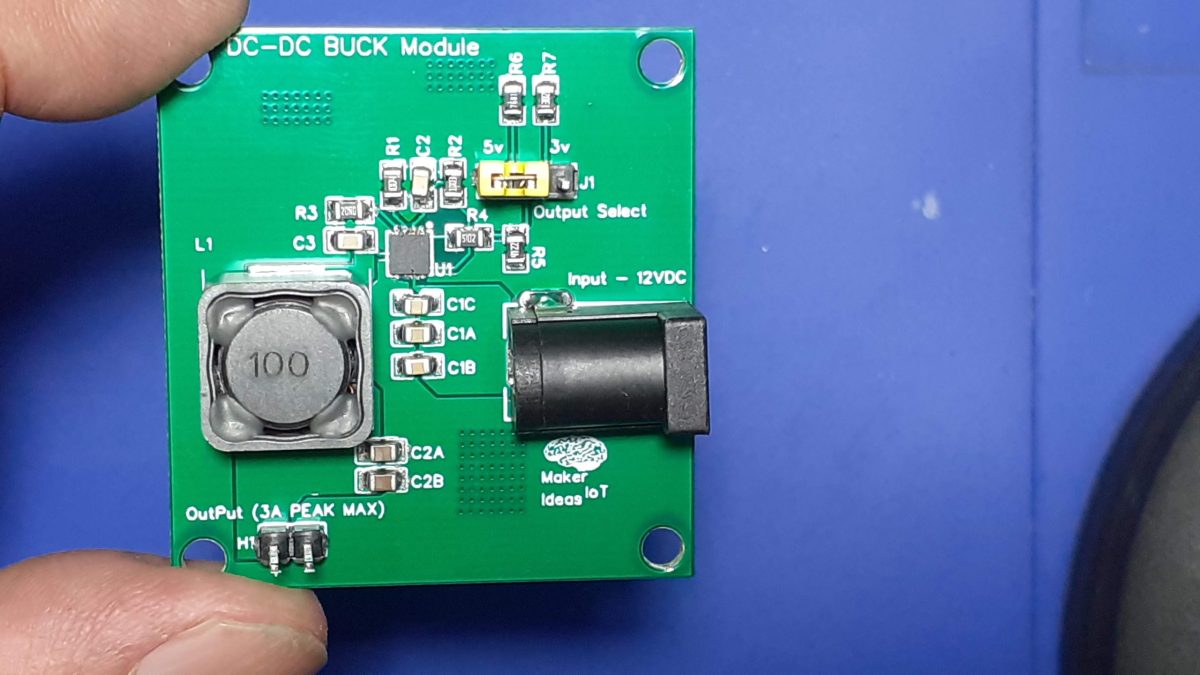
Dc-to-DC Back converters have a lot of advantages over traditional linear voltage regulator solutions. Most of these advantages are related to the smaller size of these circuits, in comparison to their linear counterparts, as well as their higher efficiency and lower power consumption to name a few.
I am by no means a power supply guy, and as such, I usually buy my power supply modules. The same also applies to boost and buck converters. I am usually quite comfortable leaving the design of these critical parts to those who actually know what they are doing.
It thus seemed like a reasonable challenge to actually try and design and build one by myself, and that will be the story behind this post.
Finding a suitable driver IC
This journey started at a very strange place. When I decided to go ahead and build this Buck converter module, I had no specific driver IC in mind. I was thus browsing through the long list of dc-to-dc- buck converters on my component suppliers’ website, randomly pulling up a datasheet to take a closer look, mainly looking for something with as few external components as possible, while also having a decent current supply capability, as well as being able to operate on an input supply of 4v to about 24v, which is well within my usual range…
I eventually settled on the MPS MP9943. Definitely not the cheapest but still affordable, and in a QFN8 package, so that I am still able to actually solder it to a PCB!
-Wide 4V to 36V Continuous Operating Input
Range
-85mΩ/55mΩ Low RDS(ON) Internal Power
MOSFETs
-High-Efficiency Synchronous Mode Operation
-410kHz Switching Frequency
-Synchronizes from 200kHz to 2.2MHz
-External Clock
-High Duty Cycle for Automotive Cold-crank
-Internal Power-Save Mode
-Internal Soft-Start
-Power Good Indicator
-Over Current Protection and Hiccup
-Thermal Shutdown
-Output Adjustable from 0.8V
-Available in an QFN-8 (3mmx3mm)
package
and with a peak current supply of up to 3A – Not too bad at all.
The actual design
As mentioned already, I am not ( or at least I don’t see myself) a power supply design expert. I believe I am perfectly capable with the linear stuff, by switchmode was never my strong point 🙂 This prototype will just be based on the recommended design in the datasheet, at least for the first version, and then, later versions may feature some customisation as actually needed.

From the picture above, we can see that there are indeed not a lot of external components required. And in my humble opinion, the efficiency vs load also seems to be quite reasonable.
I thus went ahead and started reading this datasheet in detail. I found two typical-use circuits with recommended component values, from which I build my prototype.
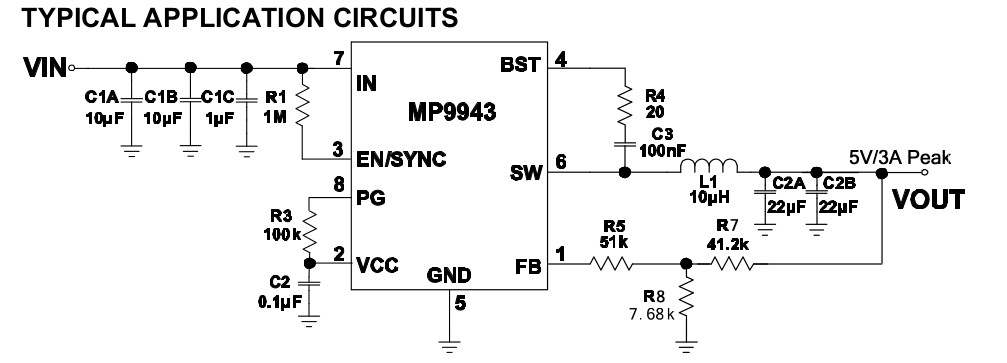
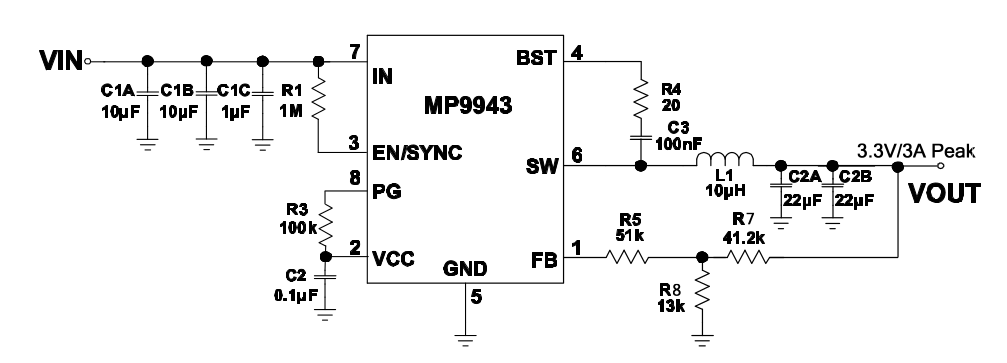
I chose to combine these two circuits to give me a variable output module, that will be selectable between 5v and 3v.
I also chose an inductor with a 6A maximum current rating, as the datasheet states that we should choose one with at least a 25% higher current rating than our peak requirement. My logic here was that 100% would be a good number, as the inductor would in theory never saturate?? as well as produce less heat etc ?? Please comment on this, as I may be barking up the wrong tree here 🙂
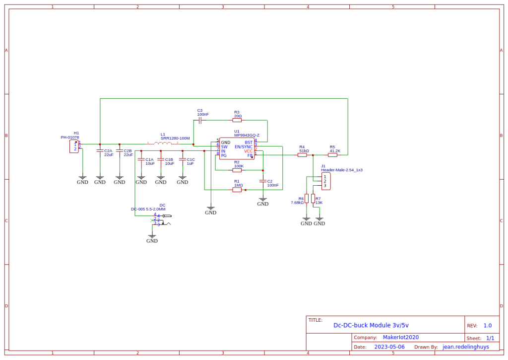
The schematic above is what I came up with. A jumper will allow the selection of the output voltage, as this is determined by the value of the resistor at R8, in my case 13K or 7.68k… I also assume that that resistor can later be replaced by a 20k trimpot or similar to give a truly variable output.
PCB Layout
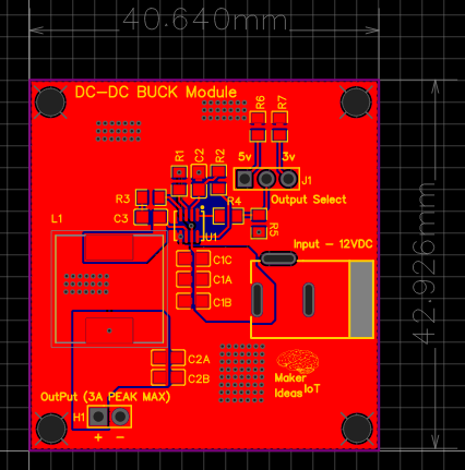
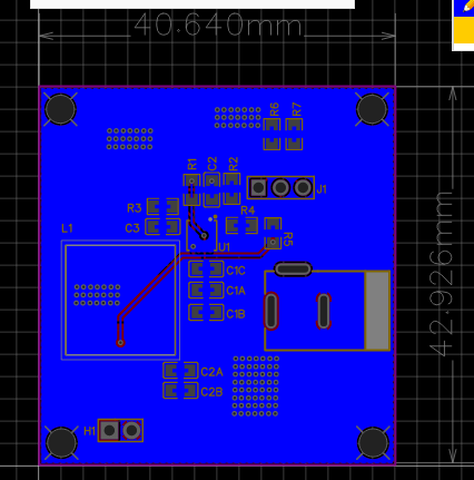
The PCB layout was an attempt to follow the datasheet recommendations as closely as possible, while still having my own design. I am also aware that I may have wasted quite a bit of space, but for now, my focus is on getting a working design. I can always try to squeeze it into a smaller space later.
Assembly
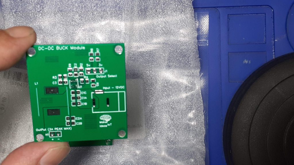
After receiving the PCBs back from the factory, and receiving the components from the supplier, I started on the assembly. While uneventful, It was worth mentioning that this project does require a stencil. The DFN-8 package is quite small (only 3mmx3mm), with eight leads, so that makes for some tiny spacing between them. As it is also a leadless package, I did not want to chance to have too much solder paste in there.
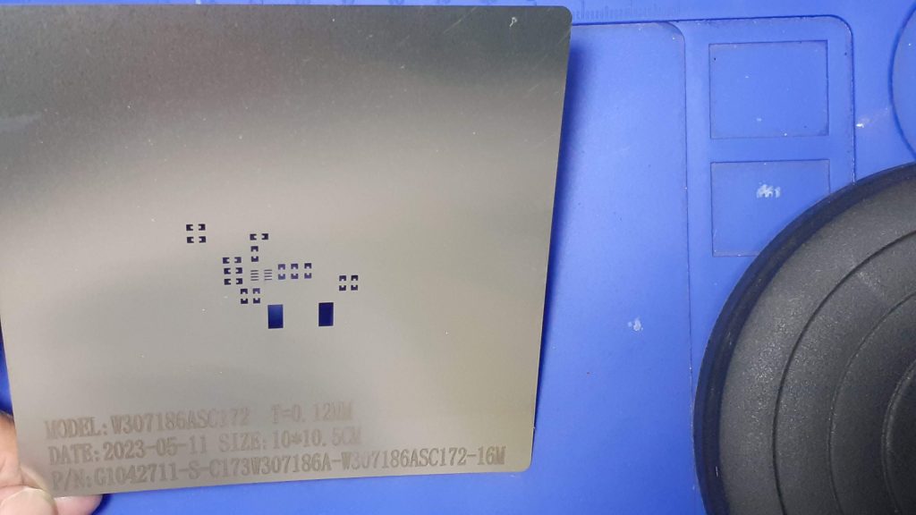
As we can clearly see in the picture above, the pads are super tiny. The other components are 0805 ( for reference).
My standard way for assembling DFN packages is to actually level the part of the PCB while reflowing the PCB with a hotplate. Then, when the solder has all melted and is in a liquid state, I carefully place the part with tweezers and remove the PCB from the hotplate.
Alternatively, I remove the PCB from the hotplate first, leaving it to cool down a bit, and then, using a hot air gun with a small nozzle, reflowing only the area where the part needs to be placed, and carefully placing it onto the melted solder.
Both of these methods seem to be working quite well, for me at least, but the hot air method does however have the risk of a bit of solder splatter, which may form unwanted bridges… The part also gets heated a bit, as it has to be held in place for a few seconds to prevent it from being blown around by the hot air.
Testing
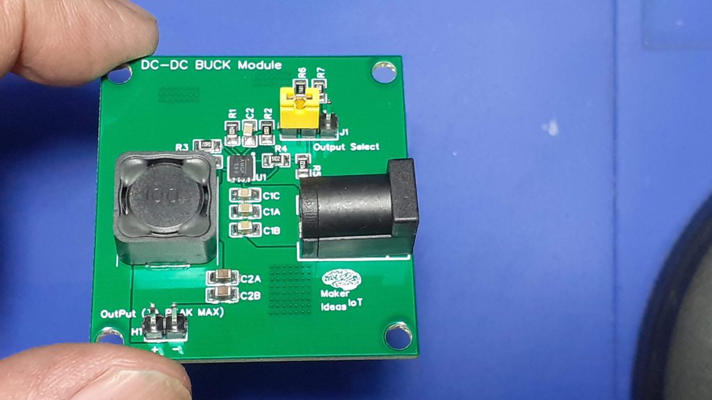
I am quite happy to report that the module works as expected, with a steady output of 3.31v and 5.08v respectively at no load.
Under load, I tested with a 1A and 2A load respectively, both voltages are also stable. Ripple, as measured by myself, and using a “not too good” digital oscilloscope, seems to be about 110mv peak-to-peak.
Using better probes, and a better scope, I may be able to get a better and more accurate reading.
Conclusion
This was quite an exciting project, with setting myself a challenge, and actually achieving what I set out to do. While I am sure that the module in its current state may actually not quite be perfect, and that it surely has a lot of room for improvement, I am satisfied with its performance, and just plainly, the fact that it actually works!
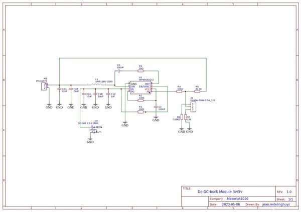
Gerber_PCB_SMPS-Module-3A-Peak_2023-05-06
*PCBWay community is a sharing platform. We are not responsible for any design issues and parameter issues (board thickness, surface finish, etc.) you choose.
Raspberry Pi 5 7 Inch Touch Screen IPS 1024x600 HD LCD HDMI-compatible Display for RPI 4B 3B+ OPI 5 AIDA64 PC Secondary Screen(Without Speaker)
BUY NOW
ESP32-S3 4.3inch Capacitive Touch Display Development Board, 800×480, 5-point Touch, 32-bit LX7 Dual-core Processor
BUY NOW
Raspberry Pi 5 7 Inch Touch Screen IPS 1024x600 HD LCD HDMI-compatible Display for RPI 4B 3B+ OPI 5 AIDA64 PC Secondary Screen(Without Speaker)
BUY NOW- Comments(0)
- Likes(0)
 Log in to post comments.
- 0 USER VOTES
- YOUR VOTE 0.00 0.00
- 1
- 2
- 3
- 4
- 5
- 6
- 7
- 8
- 9
- 10
- 1
- 2
- 3
- 4
- 5
- 6
- 7
- 8
- 9
- 10
- 1
- 2
- 3
- 4
- 5
- 6
- 7
- 8
- 9
- 10
- 1
- 2
- 3
- 4
- 5
- 6
- 7
- 8
- 9
- 10
 More by Jean Redelinghuys MakerIoT2020
-
 RA-02 Breakout with Level converters
Breadboard and beginner-friendly RA-02 Breakout ModuleMost Makers and electronics enthusiasts may al...
-
 ATMEGA328P Module with integrated LoRa and CAN Bus
ATMEGA328P Module with integrated LoRa and CAN-BUSINTRODUCTIONIn my quest to perfect my LoRa telemet...
-
 Sx127x-Ra-02-Test-Module with ATMEGA328P-AU
SX127x LoRa/FSK/OOK Prototype Radio BoardI recently had a requirement to do some automation/telemetr...
-
 USB-ASP Programmer ATMEGA8
Build your own USB-ASP Programmer CloneBymakeriot2020 FEB 21, 2022 Arduino, ASP programmerUsing mor...
-
 ATTiny1616-LIGHT-Controller-with-CAN_B_PCB_ATTiny1616-LIGHT-Controller-with-C_2024-09-11
Assembly of the ATTiny1616 Can bus controller PCBThe Assembly of the ATTiny1616 Can Bus Controller P...
-
 ATTiny1616QFN-CAN-Remote-Neopixel-Ligh_PCB_ATTiny1616QFN-CAN-Remote-Neopixel-2024-09-11_2024-09-11
NeoPixel CAN-Bus Module with local controlAs part of my current project to add NeoPixels to the cabi...
-
 PCB_MCP23008_2023-10-08
MCP23008 BreakoutI designed this breakout to assist me during prototyping my next version of the “RP...
-
 PCB_XiaoRP2040-Mouse-REV2
Xiao RP2040 Joystick Mouse – revision 2.00Revision 1.0 of the ProjectOver the last few months, I hav...
-
 Multi Purpose IO Card
Multi-Purpose IO CardWhen we are working on a prototype, we always need access to pushbuttons, encod...
-
 Variable Voltage Power Module
Powering electronics projects are always challenging. This Variable vol...
Variable Voltage Power Module
Variable Voltage Power ModulePowering electronics projects are always challenging. This Variable vol...
-
 I2C Matrix Keypad
An I2C Matrix KeypadThe completed I2C Matrix KeypadIn a previous post this month I introduced my 4×4...
-
 ESP32-S Development Board, in "Arduino Uno" form factor
UPDATE 24/06/2023:This board now has a Hardware Revision 2.0 available. It is the same board but wit...
-
 W307186ASC94_Gerber_PCB_USB-Ports
USB Power Supply ModuleUSB Ports are quite handy to power all our day-to-day electronic devices, but...
-
 Atmega 328P based PWM controller Card
ATMega 328P Based PWM controller CardAs part of my recent ESP-12E I2C Base Board project, I designed...
-
 W307186ASC71_Gerber_PCB_ESP-Now Remote
Today we will look at the remote control unit for the Robotic Toy Car – Part 6.The project is close ...
-
 W307186ASV69_Gerber_PCB_Robot-Car-MCU-Board Prototype
In our last project, we started working on repurposing an old toy car. In this part, Robot Toy Car –...
-
 W307186ASV62_Gerber_PCB_DUAL-H-Bridge
by makeriot2020 on May 27, 2022Many of us have old toys laying around the house, they belong to ou...
-
 CAN-BUS Breakout
Breadboard Compatible CAN-BUS Breakout ModuleWhat is this:Some of us have already used the commonly ...
-
 RA-02 Breakout with Level converters
Breadboard and beginner-friendly RA-02 Breakout ModuleMost Makers and electronics enthusiasts may al...
-
 ATMEGA328P Module with integrated LoRa and CAN Bus
ATMEGA328P Module with integrated LoRa and CAN-BUSINTRODUCTIONIn my quest to perfect my LoRa telemet...
-
 Sx127x-Ra-02-Test-Module with ATMEGA328P-AU
SX127x LoRa/FSK/OOK Prototype Radio BoardI recently had a requirement to do some automation/telemetr...
-
 USB-ASP Programmer ATMEGA8
Build your own USB-ASP Programmer CloneBymakeriot2020 FEB 21, 2022 Arduino, ASP programmerUsing mor...
-
 ATTiny1616-LIGHT-Controller-with-CAN_B_PCB_ATTiny1616-LIGHT-Controller-with-C_2024-09-11
Assembly of the ATTiny1616 Can bus controller PCBThe Assembly of the ATTiny1616 Can Bus Controller P...
-
 ATTiny1616QFN-CAN-Remote-Neopixel-Ligh_PCB_ATTiny1616QFN-CAN-Remote-Neopixel-2024-09-11_2024-09-11
NeoPixel CAN-Bus Module with local controlAs part of my current project to add NeoPixels to the cabi...
-
 PCB_MCP23008_2023-10-08
MCP23008 BreakoutI designed this breakout to assist me during prototyping my next version of the “RP...
-
 PCB_XiaoRP2040-Mouse-REV2
Xiao RP2040 Joystick Mouse – revision 2.00Revision 1.0 of the ProjectOver the last few months, I hav...
-
 Multi Purpose IO Card
Multi-Purpose IO CardWhen we are working on a prototype, we always need access to pushbuttons, encod...
-
 Variable Voltage Power Module
Powering electronics projects are always challenging. This Variable vol...
Variable Voltage Power Module
Variable Voltage Power ModulePowering electronics projects are always challenging. This Variable vol...
-
 I2C Matrix Keypad
An I2C Matrix KeypadThe completed I2C Matrix KeypadIn a previous post this month I introduced my 4×4...
-
 ESP32-S Development Board, in "Arduino Uno" form factor
UPDATE 24/06/2023:This board now has a Hardware Revision 2.0 available. It is the same board but wit...
-
-
-
Modifying a Hotplate to a Reflow Solder Station
948 1 6 -
MPL3115A2 Barometric Pressure, Altitude, and Temperature Sensor
479 0 1 -
-
Nintendo 64DD Replacement Shell
410 0 2 -
V2 Commodore AMIGA USB-C Power Sink Delivery High Efficiency Supply Triple Output 5V ±12V OLED display ATARI compatible shark 100W
1188 4 2 -
How to measure weight with Load Cell and HX711
734 0 3


